ZHCSOX1 October 2020 OPA455
PRODUCTION DATA
- 1 特性
- 2 应用
- 3 说明
- 4 Revision History
- 5 Pin Configuration and Functions
- 6 Specifications
- 7 Detailed Description
- 8 Application and Implementation
- 9 Power Supply Recommendations
- 10Layout
- 11Device and Documentation Support
- 12Mechanical, Packaging, and Orderable Information
8.2.1.2 Detailed Design Procedure
Figure 8-1 shows a noninverting circuit with a moderately high closed-loop gain (AV) of 14 V/V (22.9 dB). In this example, a 5-VPK ac signal is amplified to 70 VPK across a 10-kΩ load resistor connected to the output. The peak current for this application is 8.5 mA, and is well within the OPA455 output current capability. Higher output current, typically up to 30 mA, may be attained at the expense of the output swing to the supply rails.
The noninverting amplifier circuit shows the OPA455 enable-disable function. When placed in disabled mode, the op amp becomes nonfunctional, and the current consumption is reduced to approximately one-third to one-half of the enabled level. An enable active state occurs when the E/D pin is left open, or is biased 3 V to 5 V greater than the E/D Com voltage level. If biased between the E/D com level, to E/D Com + 0.65 V, the OPA455 disables. More information about this function is provided in the Enable and Disable section.
Op amps designed for high-voltage and high-power applications may encounter output loads that can be quite different than those used in low-voltage, low-power, op-amp applications. Although every effort is made to make a high-voltage op amp such as the OPA455 robust and tolerant of different supply and different output load conditions, some loads can present potentially harmful circumstances.
Purely resistive output loads operating within the current capability range of the OPA455 do not present an unsafe condition, provided the thermal requirements discussed in the Layout section. Complex loads that have inductive or capacitive reactive elements might present an unsafe condition, and must be fully considered and addressed before implementation.
A potentially destructive mechanism is the back EMF transient that can be generated when driving an inductive load. D1, D2, Z1 and Z2 in the noninverting crcuit drawing have been added to the basic OPA455 amplifier circuit to provide protection in the event of back EMF. If the voltage at the OPA455 output attempts to momentarily rise above V+, D1 becomes forward-biased and clamps the voltage between the output and V+ pins. This clamp must be sufficient to protect the OPA455 output transistor. If the event causes the V+ voltage to increase the power supply bypass capacitor, Z1, or both, a Zener diode or a transient voltage suppressor (TVS) can provide a path for the transient current to ground. D2 and Z2 provide the same protection in the negative supply circuit.
The OPA455 noninverting amplifier circuit with a closed-loop gain of 14 V/V has a small-signal, –3-dB bandwidth of nearly 800 kHz. However, the large-signal bandwidth is likely of greater importance in a high-output-voltage application. For that mode of operation, the slew rate of the op amp and the peak output swing voltage must be considered in order to determine the maximum large-signal bandwidth. The slew rate (SR) of the OPA455 is typically 6.5 V/µs, or 6.5 × 10⁶ V/s. Using the 70-VPK output voltage available from the noninverting circuit drawing, the maximum large-signal bandwidth is calculated from the slew rate formula. Equation 1, Equation 2 and Equation 3 show the calculation process.

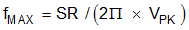

where
- SR = 6.5 × 10⁶ V/s
- VPK = 85 V
The best design practice for when a typical specification, such as slew rate, is used for calculation is to allow for variability in the actual value of the specification because of device manufacturing variations. In this example, keeping the large signal fMAX to 10 kHz is sufficient to make sure the output avoids slew rate limiting.