ZHCSOX1 October 2020 OPA455
PRODUCTION DATA
- 1 特性
- 2 应用
- 3 说明
- 4 Revision History
- 5 Pin Configuration and Functions
- 6 Specifications
- 7 Detailed Description
- 8 Application and Implementation
- 9 Power Supply Recommendations
- 10Layout
- 11Device and Documentation Support
- 12Mechanical, Packaging, and Orderable Information
7.3.4 Enable and Disable
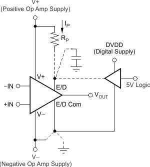
If left disconnected, the E/D Com pin is pulled near V– (negative supply) by an internal 10-μA current source. When left floating, the E/D pin is held approximately 2 V above E/D Com by an internal 1-µA source. Even though active operation of the OPA455 results when the E/D and E/D Com pins are not connected, a moderately fast, negative-going signal capacitively coupled to the E/D pin can overpower the 1-µA pullup current and cause device shutdown. This behavior can appear as an oscillation and is encountered first near extreme cold temperatures. If the enable function is not used, a conservative approach is to connect E/D through a 30-pF capacitor to a low impedance source. Another alternative is the connection of an external current source from V+ (positive supply) sufficient enough to hold the enable level above the shutdown threshold. Figure 7-1 shows a circuit that connects E/D and E/D Com. The E/D Com pin is limited to (V–) + 100 V to enable the use of digital ground in a application where the OPA455 power supply is ±75 V.
When the E/D pin is dropped to a voltage between 0 V and 0.65 V above the E/D Com pin voltage, the output of the OPA455 becomes disabled. While in this state, the impedance of the output increases to approximately 160 kΩ. Because the inputs are still active, an input signal might be passed to the output of the amplifier. The voltage at the amplifier output is reduced because of a drop across this output impedance, and may appear distorted compared to a normal operation output.
After the E/D pin voltage is raised to a voltage between 2.5 V and 5 V greater than the E/D Com, the output impedance returns to a normal state, and the amplifier operates normally.
 Figure 7-1 E/D and
E/D Com