ZHCSJY2A June   2019  – September 2019 OPA2834

PRODUCTION DATA.  

  1. 特性
  2. 应用
  3. 说明
    1.     Device Images
      1.      1kHz FFT 图(VOUT = 1VRMS,RL = 100kΩ,G = 1)
      2.      低侧电流分流监控
  4. 修订历史记录
  5. Device Comparison Table
  6. Pin Configuration and Functions
    1.     Pin Functions
  7. Specifications
    1. 7.1 Absolute Maximum Ratings
    2. 7.2 ESD Ratings
    3. 7.3 Recommended Operating Conditions
    4. 7.4 Thermal Information
    5. 7.5 Electrical Characteristics: 3V to 5V
    6. 7.6 Typical Characteristics: Vs = 5 V
    7. 7.7 Typical Characteristics: VS = 3.0 V
    8. 7.8 Typical Characteristics: ±2.5-V to ±1.5-V Split Supply
  8. Detailed Description
    1. 8.1 Overview
    2. 8.2 Functional Block Diagrams
    3. 8.3 Feature Description
      1. 8.3.1 Input Common-Mode Voltage Range
      2. 8.3.2 Output Voltage Range
      3. 8.3.3 Low-Power Applications and the Effects of Resistor Values on Bandwidth
      4. 8.3.4 Driving Capacitive Loads
    4. 8.4 Device Functional Modes
      1. 8.4.1 Split-Supply Operation (±1.35 V to ±2.7 V)
      2. 8.4.2 Single-Supply Operation (2.7 V to 5.4 V)
  9. Application and Implementation
    1. 9.1 Application Information
      1. 9.1.1 Noninverting Amplifier
      2. 9.1.2 Inverting Amplifier
    2. 9.2 Typical Applications
      1. 9.2.1 Low-Side Current Sensing
        1. 9.2.1.1 Design Requirements
        2. 9.2.1.2 Detailed Design Procedure
      2. 9.2.2 Field Transmitter Sensor Interface
      3. 9.2.3 Ultrasonic Flow Meters
      4. 9.2.4 Microphone Pre-Amplifier
  10. 10Power Supply Recommendations
  11. 11Layout
    1. 11.1 Layout Guidelines
    2. 11.2 Layout Examples
  12. 12器件和文档支持
    1. 12.1 文档支持
      1. 12.1.1 相关文档
    2. 12.2 接收文档更新通知
    3. 12.3 社区资源
    4. 12.4 商标
    5. 12.5 静电放电警告
    6. 12.6 Glossary
  13. 13机械、封装和可订购信息

封装选项

机械数据 (封装 | 引脚)
散热焊盘机械数据 (封装 | 引脚)
订购信息

Driving Capacitive Loads

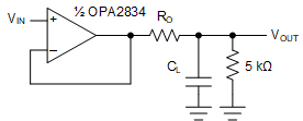
The OPA2834 drives up to a nominal capacitive load of 10 pF on the output with no special consideration and without the need of RO. When driving capacitive loads greater than 10 pF, TI recommends using a small resistor (RO) in series with the output as close to the device as possible. Without RO, output capacitance interacts with the output impedance (ZO) of the amplifier causing phase shift in the feedback loop of the amplifier reducing the phase margin. This reduction in the phase margin causes peaking in the frequency response and overshoot and ringing in the pulse response. Interaction with other parasitic elements can lead to further instability or ringing. Inserting RO isolates the phase shift from the loop gain path and restores the phase margin; however RO can limit the bandwidth slightly. Figure 49 shows a diagram of driving capacitive loads.

Figure 39 shows the test circuit and shows the recommended values of RO versus capacitive loads, CL. See Figure 40 for the frequency responses with various optimized values of RO with CL.
OPA2834 Capacitor_Drive_Section.gifFigure 49. Driving Capacitive Loads With the OPA2834