ZHCSA42F August 2010 – September 2020 MSP430F5333 , MSP430F5335 , MSP430F5336 , MSP430F5338
PRODUCTION DATA
- 1 特性
- 2 应用
- 3 说明
- 4 功能方框图
- 5 Revision History
- 6 Device Comparison
- 7 Terminal Configuration and Functions
-
8 Specifications
- 8.1 Absolute Maximum Ratings
- 8.2 ESD Ratings
- 8.3 Recommended Operating Conditions
- 8.4 Active Mode Supply Current Into VCC Excluding External Current
- 8.5 Low-Power Mode Supply Currents (Into VCC) Excluding External Current
- 8.6 Thermal Resistance Characteristics
- 8.7 Schmitt-Trigger Inputs – General-Purpose I/O
- 8.8 Inputs – Ports P1, P2, P3, and P4
- 8.9 Leakage Current – General-Purpose I/O
- 8.10 Outputs – General-Purpose I/O (Full Drive Strength)
- 8.11 Outputs – General-Purpose I/O (Reduced Drive Strength)
- 8.12 Output Frequency – Ports P1, P2, and P3
- 8.13 Typical Characteristics – Outputs, Reduced Drive Strength (PxDS.y = 0)
- 8.14 Typical Characteristics – Outputs, Full Drive Strength (PxDS.y = 1)
- 8.15 Crystal Oscillator, XT1, Low-Frequency Mode
- 8.16 Crystal Oscillator, XT2
- 8.17 Internal Very-Low-Power Low-Frequency Oscillator (VLO)
- 8.18 Internal Reference, Low-Frequency Oscillator (REFO)
- 8.19 DCO Frequency
- 8.20 PMM, Brownout Reset (BOR)
- 8.21 PMM, Core Voltage
- 8.22 PMM, SVS High Side
- 8.23 PMM, SVM High Side
- 8.24 PMM, SVS Low Side
- 8.25 PMM, SVM Low Side
- 8.26 Wake-up Times From Low-Power Modes and Reset
- 8.27 Timer_A, Timers TA0, TA1, and TA2
- 8.28 Timer_B, Timer TB0
- 8.29 Battery Backup
- 8.30 USCI (UART Mode)
- 8.31 USCI (SPI Master Mode)
- 8.32 USCI (SPI Slave Mode)
- 8.33 USCI (I2C Mode)
- 8.34 12-Bit ADC, Power Supply and Input Range Conditions
- 8.35 12-Bit ADC, Timing Parameters
- 8.36 12-Bit ADC, Linearity Parameters Using an External Reference Voltage
- 8.37 12-Bit ADC, Linearity Parameters Using AVCC as Reference Voltage
- 8.38 12-Bit ADC, Linearity Parameters Using the Internal Reference Voltage
- 8.39 12-Bit ADC, Temperature Sensor and Built-In VMID
- 8.40 REF, External Reference
- 8.41 REF, Built-In Reference
- 8.42 12-Bit DAC, Supply Specifications
- 8.43 12-Bit DAC, Linearity Specifications
- 8.44 12-Bit DAC, Output Specifications
- 8.45 12-Bit DAC, Reference Input Specifications
- 8.46 12-Bit DAC, Dynamic Specifications
- 8.47 12-Bit DAC, Dynamic Specifications (Continued)
- 8.48 Comparator_B
- 8.49 Ports PU.0 and PU.1
- 8.50 LDO-PWR (LDO Power System)
- 8.51 Flash Memory
- 8.52 JTAG and Spy-Bi-Wire Interface
-
9 Detailed Description
- 9.1 Overview
- 9.2 CPU
- 9.3 Instruction Set
- 9.4 Operating Modes
- 9.5 Interrupt Vector Addresses
- 9.6 Memory
- 9.7 Bootloader (BSL)
- 9.8 JTAG Operation
- 9.9 Flash Memory
- 9.10 RAM
- 9.11 Backup RAM
- 9.12
Peripherals
- 9.12.1 Digital I/O
- 9.12.2 Port Mapping Controller
- 9.12.3 Oscillator and System Clock
- 9.12.4 Power-Management Module (PMM)
- 9.12.5 Hardware Multiplier (MPY) (Link to User's Guide)
- 9.12.6 Real-Time Clock (RTC_B)
- 9.12.7 Watchdog Timer (WDT_A)
- 9.12.8 System Module (SYS)
- 9.12.9 DMA Controller
- 9.12.10 Universal Serial Communication Interface (USCI)
- 9.12.11 Timer TA0
- 9.12.12 Timer TA1
- 9.12.13 Timer TA2
- 9.12.14 Timer TB0
- 9.12.15 Comparator_B
- 9.12.16 ADC12_A
- 9.12.17 DAC12_A
- 9.12.18 CRC16
- 9.12.19 Voltage Reference (REF) Module
- 9.12.20 LDO and PU Port
- 9.12.21 Embedded Emulation Module (EEM)
- 9.12.22 Peripheral File Map
- 9.13
Input/Output Diagrams
- 9.13.1 Port P1 (P1.0 to P1.7) Input/Output With Schmitt Trigger
- 9.13.2 Port P2 (P2.0 to P2.7) Input/Output With Schmitt Trigger
- 9.13.3 Port P3 (P3.0 to P3.7) Input/Output With Schmitt Trigger
- 9.13.4 Port P4 (P4.0 to P4.7) Input/Output With Schmitt Trigger
- 9.13.5 Port P5 (P5.0 and P5.1) Input/Output With Schmitt Trigger
- 9.13.6 Port P5 (P5.2 to P5.7) Input/Output With Schmitt Trigger
- 9.13.7 Port P6 (P6.0 to P6.7) Input/Output With Schmitt Trigger
- 9.13.8 Port P7 (P7.2) Input/Output With Schmitt Trigger
- 9.13.9 Port P7 (P7.3) Input/Output With Schmitt Trigger
- 9.13.10 Port P7 (P7.4 to P7.7) Input/Output With Schmitt Trigger
- 9.13.11 Port P8 (P8.0 to P8.7) Input/Output With Schmitt Trigger
- 9.13.12 Port P9 (P9.0 to P9.7) Input/Output With Schmitt Trigger
- 9.13.13 Port PU (PU.0 and PU.1) Ports
- 9.13.14 Port PJ (PJ.0) JTAG Pin TDO, Input/Output With Schmitt Trigger or Output
- 9.13.15 Port PJ (PJ.1 to PJ.3) JTAG Pins TMS, TCK, TDI/TCLK, Input/Output With Schmitt Trigger or Output
- 9.14 Device Descriptors
- 10Device and Documentation Support
- 11Mechanical, Packaging, and Orderable Information
9.13.13 Port PU (PU.0 and PU.1) Ports
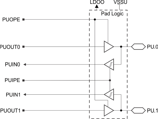
Figure 9-14 shows the pin diagram. Table 9-60 summarizes how to select the pin function.
 Figure 9-14 Port PU (PU.0 and PU.1) Diagram
Table 9-60 Port PU.0 and PU.1 Functions
| PUIPE(1) | PUOPE | PUOUT1 | PUOUT0 | PU.1 | PU.0 | PORT U FUNCTION |
|---|---|---|---|---|---|---|
| 0 | 1 | 0 | 0 | Output low | Output low | Outputs enabled |
| 0 | 1 | 0 | 1 | Output low | Output high | Outputs enabled |
| 0 | 1 | 1 | 0 | Output high | Output low | Outputs enabled |
| 0 | 1 | 1 | 1 | Output high | Output high | Outputs enabled |
| 1 | 0 | X | X | Input enabled | Input enabled | Inputs enabled |
| 0 | 0 | X | X | Hi-Z | Hi-Z | Outputs and inputs disabled |
(1) PU.1 and PU.0 inputs and outputs are supplied from LDOO. LDOO can be generated by the device using the integrated 3.3-V LDO when enabled. LDOO can also be supplied externally when the 3.3-V LDO is not being used and is disabled.