at operating temperature TJ
= 25°C, VIN = VOUT(NOM) + 1.0V or 2.5V (whichever is greater),
IOUT = 1mA, ON/OFF pin tied to VIN,
CIN = 1.0µF, and COUT = 4.7µF (unless otherwise noted)
 Figure 7-4 Short-Circuit Current (Legacy Chip) at VIN = 6V
 Figure 7-6 Short-Circuit Current (Legacy Chip) at VIN = 16V
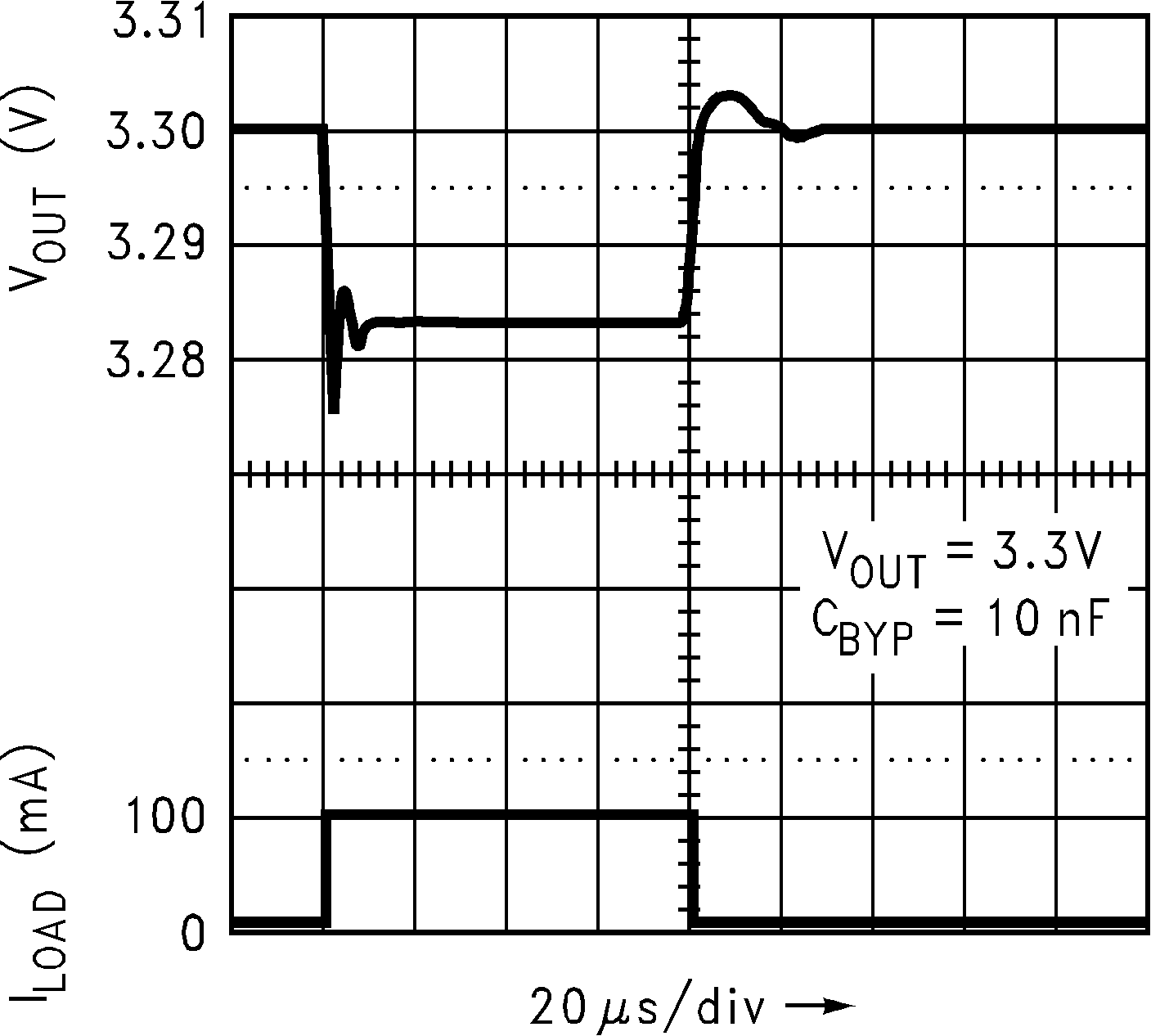
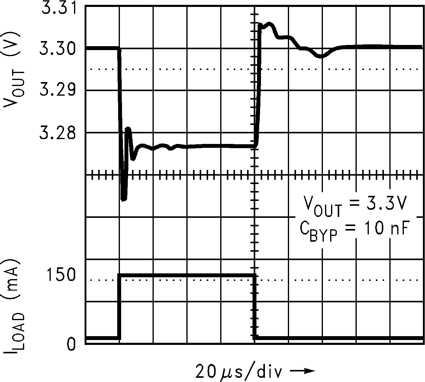
 Figure 7-8 Load
Transient Response (Legacy Chip)
 Figure 7-10 Load
Transient Response (Legacy Chip)
 Figure 7-12 Load
Transient Response (Legacy Chip)
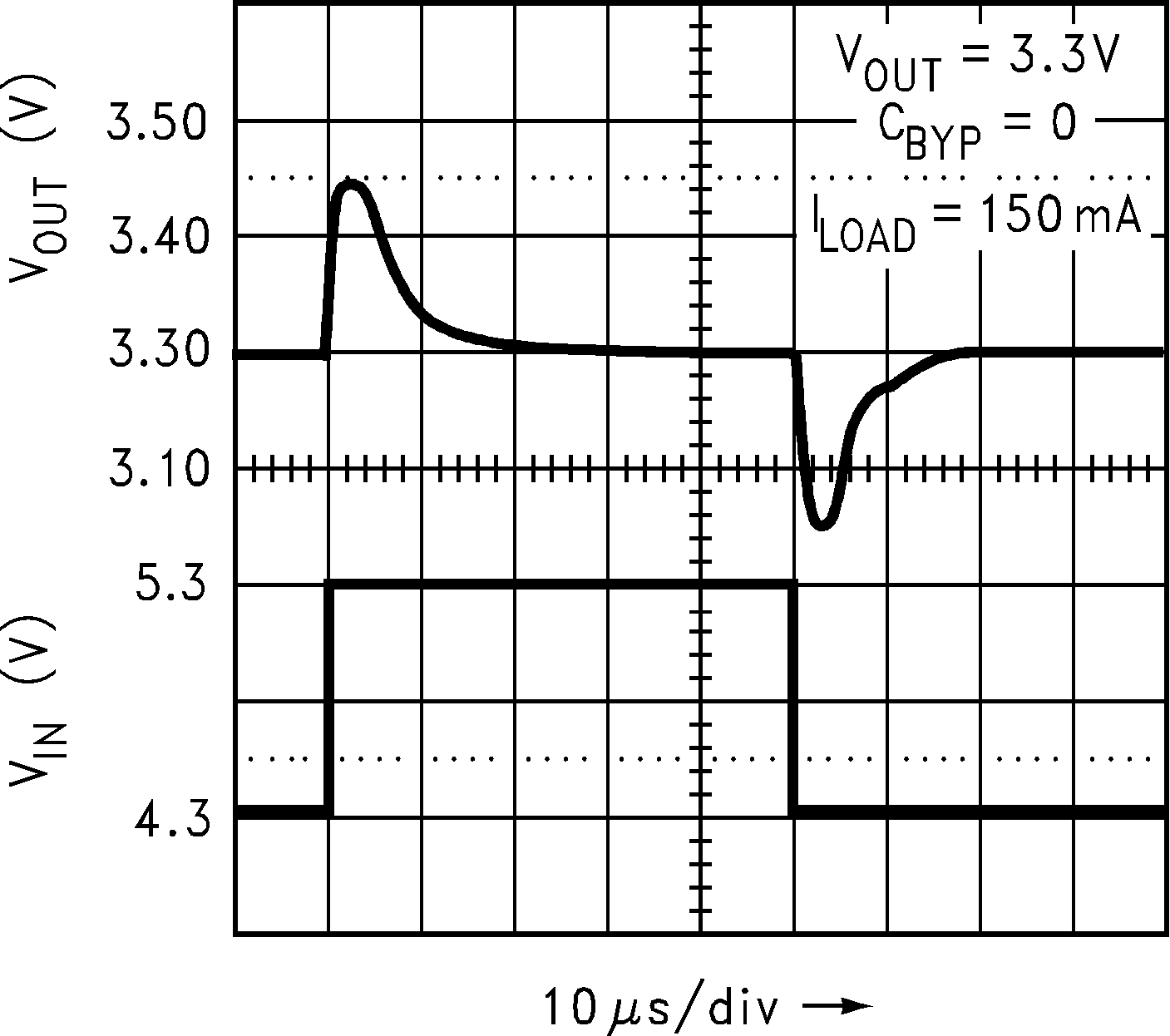
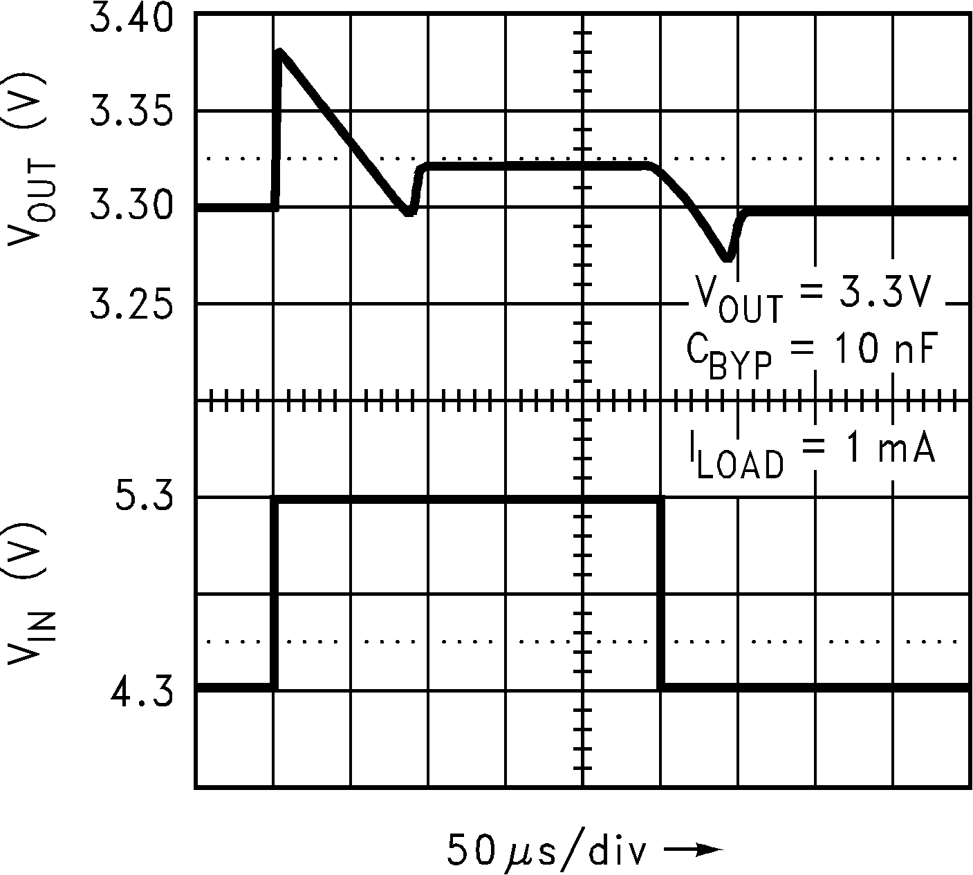
 Figure 7-14 Line
Transient Response (Legacy Chip)
 Figure 7-16 Line
Transient Response (Legacy Chip)
 Figure 7-18 Line
Transient Response (Legacy Chip)
 Figure 7-20 Line
Transient Response (Legacy Chip)
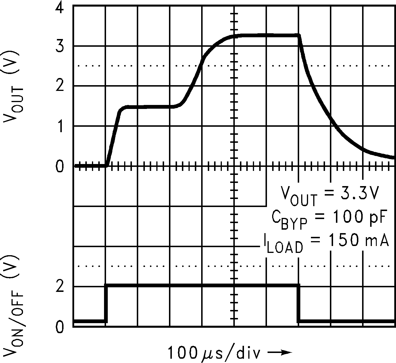
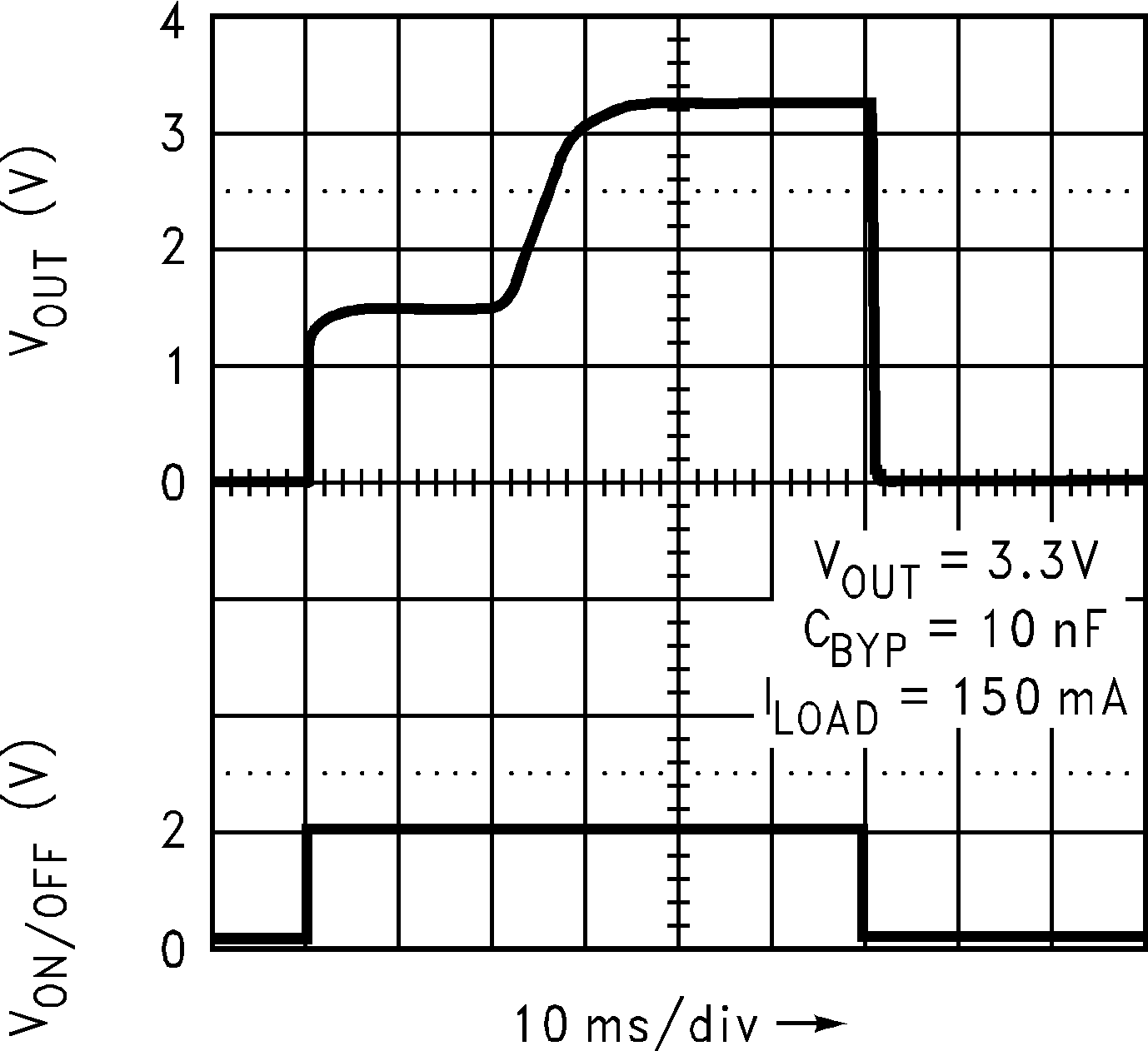
 Figure 7-22 Turn-On Time (Legacy Chip)
 Figure 7-24 Turn-On Time (Legacy Chip)
 Figure 7-26 Turn-On Time (Legacy Chip)
 Figure 7-28 Turn-On Time (Legacy Chip)
 Figure 7-5 Short-Circuit Current (New
Chip) at VIN = 6V
 Figure 7-7 Short-Circuit Current (New
Chip) at VIN = 16V
 Figure 7-9 Load Transient Response
(New Chip)
 Figure 7-11 Load Transient (New
Chip)
 Figure 7-13 Load Transient Response
(New Chip)
VOUT = 3.3V, CBYP = 0nF,
ΔVIN = 1V, IOUT = 1mA,
dV/dt = 1V/μF |
Figure 7-15 Line Transient Response
(New Chip)
VOUT = 3.3V, CBYP = 0nF,
ΔVIN = 1V, IOUT = 150mA,
dV/dt = 1V/μF |
Figure 7-17 Line Transient Response
(New Chip)
VOUT = 3.3V, CBYP = 10nF,
ΔVIN = 1V, IOUT = 1mA,
dV/dt = 1V/μF |
Figure 7-19 Line Transient Response
(New Chip)
VOUT = 3.3V, CBYP = 10nF,
ΔVIN = 1V, IOUT = 150mA,
dV/dt = 1V/μF |
Figure 7-21 Line Transient Response
(New Chip) Figure 7-23 Turn-On Time (New
Chip)
 Figure 7-25 Turn-On Time (New
Chip)
 Figure 7-27 Turn-On Time (New
Chip)
 Figure 7-29 Turn-On Time (New
Chip)

