ZHCSS00AB March 2000 – June 2025 LP2985-N
PRODUCTION DATA
- 1
- 1 特性
- 2 应用
- 3 说明
- 4 Pin Configuration and Functions
- 5 Specifications
- 6 Detailed Description
-
7 Application and Implementation
- 7.1 Application Information
- 7.2 Typical Application
- 7.3 Power Supply Recommendations
- 7.4 Layout
- 8 器件和文档支持
- 9 Revision History
- 10Mechanical, Packaging, and Orderable Information
7.1.3 Output Capacitor Requirements
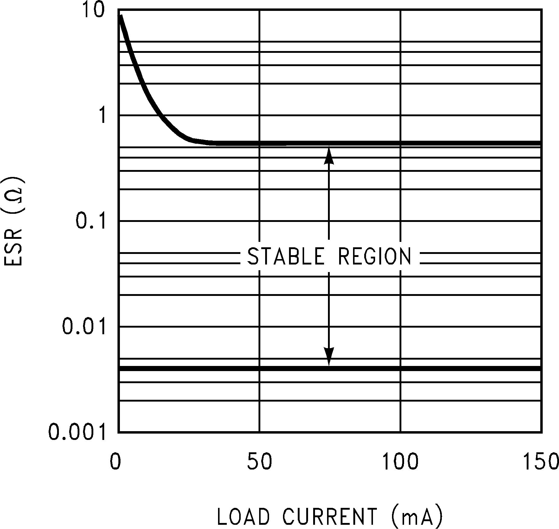
The LP2985-N (legacy chip) is designed specifically to work with ceramic output capacitors, using circuitry which allows the regulator to be stable across the entire range of output current with an output capacitor whose ESR is as low as 5mΩ. Using tantalum or film capacitors is also possible at the output, but these are not as attractive for reasons of size and cost (see the Recommended Capacitors (Legacy Chip) section). The output capacitor must meet the requirement for minimum amount of capacitance and also have an ESR value which is within the stable range. Curves are provided which show the stable ESR range as a function of load current (see Figure 7-1).
 Figure 7-1 ESR Graph (Legacy Chip)
The output capacitor must maintain the ESR within the stable region over the full operating temperature range of the application to provide stability.
The LP2985-N requires a minimum of 2.2µF on the output (output capacitor size can be increased without limit).
Remember that capacitor tolerance and variation with temperature must be taken into consideration when selecting an output capacitor so that the minimum required amount of output capacitance is provided over the full operating temperature range. Ceramic capacitors can exhibit large changes in capacitance with temperature (see the Recommended Capacitors (Legacy Chip) section). The output capacitor must be located not more than 1cm from the output pin and returned to a clean analog ground.
For the new chip, dynamic performance of the device is improved with the use of an output capacitor. Use an output capacitor within the range specified in the Recommended Operating Conditions table for stability.