ZHCS566I February 2010 – March 2022 LMZ12010
PRODUCTION DATA
- 1 特性
- 2 应用
- 3 说明
- 4 Revision History
- 5 Pin Configuration and Functions
- 6 Specifications
- 7 Detailed Description
- 8 Application and Implementation
- 9 Power Supply Recommendations
- 10Layout
- 11Device and Documentation Support
- 12Mechanical, Packaging, and Orderable Information
10.3 Power Dissipation and Thermal Considerations
When calculating module dissipation, use the maximum input voltage and the average output current for the application. Many common operating conditions are provided in the characteristic curves such that less common applications can be derived through interpolation. In all designs, the junction temperature must be kept below the rated maximum of 125°C.
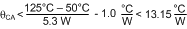
For the design case of VIN = 12 V, VOUT = 3.3 V, IOUT = 10 A, and TA-MAX = 50°C, the module must see a thermal resistance from case to ambient (θCA) of less than:
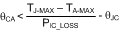
Given the typical thermal resistance from junction to case (θJC) to be 1.0°C/W. Use the 85°C power dissipation curves in Section 6.6 to estimate the PIC-LOSS for the application being designed. In this application it is 5.3 W.
To reach θCA = 13.15, the PCB is required to dissipate heat effectively. With no airflow and no external heat-sink, a good estimate of the required board area covered by 2-oz. copper on both the top and bottom metal layers is:
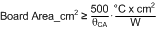
As a result, approximately 38.02 square cm of 2-oz. copper on top and bottom layers is the minimum required area for the example PCB design. This is a 6.16-cm × 6.16-cm (2.42-in × 2.42-in) square. The PCB copper heat sink must be connected to the exposed pad. For best performance, use approximately 100 8-mil thermal vias spaced 59 mil (1.5 mm) apart connect the top copper to the bottom copper.
Another way to estimate the temperature rise of a design is using θJA. An estimate of θJA for varying heat sinking copper areas and airflows can be found in the typical applications curves. If our design required the same operating conditions as before but had 225 LFPM of airflow. The required θJA is located:
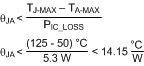
On the θJA vs copper heatsinking curve, the copper area required for this application is now only two square inches. The airflow reduced the required heat sinking area by a factor of three.
To reduce the heat sinking copper area further, this package is compatible with D3-PAK surface mount heat sinks.
For an example of a high thermal performance PCB layout for SIMPLE SWITCHER power modules, refer to the following:
- AN-2093 LMZ23610/8/6 and LMZ22010/8/6 Current Sharing Evaluation Board user's guide
- AN-2084 LMZ1420xEXT / LMZ1200xEXT Evaluation Board user's guide
- Step-Down DC-DC Converter with Integrated Low Dropout Regulator and Startup Mode data sheet
- AN-2020 Thermal Design By Insight, Not Hindsight application report
- AN-2026 Effect of PCB Design on Thermal Performance of SIMPLE SWITCHER Modules application report