ZHCS566I February   2010  – March 2022 LMZ12010

PRODUCTION DATA  

  1. 特性
  2. 应用
  3. 说明
  4. Revision History
  5. Pin Configuration and Functions
  6. Specifications
    1. 6.1 Absolute Maximum Ratings
    2. 6.2 ESD Ratings
    3. 6.3 Recommended Operating Conditions
    4. 6.4 Thermal Information
    5. 6.5 Electrical Characteristics
    6. 6.6 Typical Characteristics
  7. Detailed Description
    1. 7.1 Overview
    2. 7.2 Functional Block Diagram
    3. 7.3 Feature Description
      1. 7.3.1 Output Overvoltage Protection
      2. 7.3.2 Current Limit
      3. 7.3.3 Thermal Protection
      4. 7.3.4 Prebiased Start-Up
    4. 7.4 Device Functional Modes
      1. 7.4.1 Discontinuous Conduction and Continuous Conduction Modes
  8. Application and Implementation
    1. 8.1 Application Information
    2. 8.2 Typical Application
      1. 8.2.1 Design Requirements
      2. 8.2.2 Detailed Design Procedure
        1. 8.2.2.1 Enable Divider, RENT, RENB, and RENH Selection
        2. 8.2.2.2 Output Voltage Selection
        3. 8.2.2.3 Soft-Start Capacitor Selection
        4. 8.2.2.4 Tracking Supply Divider Option
        5. 8.2.2.5 COUT Selection
        6. 8.2.2.6 CIN Selection
      3. 8.2.3 Application Curves
  9. Power Supply Recommendations
  10. 10Layout
    1. 10.1 Layout Guidelines
    2. 10.2 Layout Examples
    3. 10.3 Power Dissipation and Thermal Considerations
    4. 10.4 Power Module SMT Guidelines
  11. 11Device and Documentation Support
    1. 11.1 Device Support
      1. 11.1.1 第三方产品免责声明
      2. 11.1.2 Development Support
    2. 11.2 Documentation Support
      1. 11.2.1 Related Documentation
    3. 11.3 支持资源
    4. 11.4 接收文档更新通知
    5. 11.5 Trademarks
    6. 11.6 Electrostatic Discharge Caution
    7. 11.7 术语表
  12. 12Mechanical, Packaging, and Orderable Information

封装选项

机械数据 (封装 | 引脚)
散热焊盘机械数据 (封装 | 引脚)
订购信息

Discontinuous Conduction and Continuous Conduction Modes

At light load, the regulator will operate in discontinuous conduction mode (DCM). With load currents above the critical conduction point, it will operate in continuous conduction mode (CCM). When operating in DCM, inductor current is maintained to an average value equaling IOUT. In DCM, the low-side switch will turn off when the inductor current falls to zero. This causes the inductor current to resonate. Although it is in DCM, the current is allowed to go slightly negative to charge the bootstrap capacitor.

In CCM, current flows through the inductor through the entire switching cycle and never falls to zero during the off time.

Figure 7-2 is a comparison pair of waveforms showing both the CCM (upper) and DCM operating modes.

GUID-78ACC0BE-045A-4864-90B5-07E4D6E36C5D-low.png
VIN = 12 V, VO = 3.3 V, IO = 3 A / 0.3 A
Figure 7-2 CCM and DCM Operating Modes

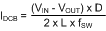
The approximate formula for determining the DCM/CCM boundary is:

Equation 1. GUID-00F958A3-CCEA-4156-AF7D-0CF439DA4A81-low.gif

The inductor internal to the module is 2.2 μH. This value was chosen as a good balance between low and high input voltage applications. The main parameter affected by the inductor is the amplitude of the inductor ripple current (ΔiL). ΔiL can be calculated with:
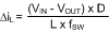
Equation 2. GUID-D8C6CE90-2869-4D4B-8CDD-20C78E5D0BEC-low.gif

where

  • VIN is the maximum input voltage.
  • fSW is typically 359 kHz.

If the output current IOUT is determined by assuming that IOUT = IL, the higher and lower peak of ΔiL can be determined.