ZHCS566I February 2010 – March 2022 LMZ12010
PRODUCTION DATA
- 1 特性
- 2 应用
- 3 说明
- 4 Revision History
- 5 Pin Configuration and Functions
- 6 Specifications
- 7 Detailed Description
- 8 Application and Implementation
- 9 Power Supply Recommendations
- 10Layout
- 11Device and Documentation Support
- 12Mechanical, Packaging, and Orderable Information
8.2.2.6 CIN Selection
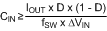
The LMZ12010 module contains two internal ceramic input capacitors. Additional input capacitance is required external to the module to handle the input ripple current of the application. The input capacitor can be several capacitors in parallel. This input capacitance must be located in very close proximity to the module. Input capacitor selection is generally directed to satisfy the input ripple current requirements rather than by capacitance value. Input ripple current rating is dictated by Equation 12:

where
- D ≊ VOUT / VIN
As a point of reference, the worst case ripple current will occur when the module is presented with full load current and when VIN = 2 × VOUT.
Recommended minimum input capacitance is 30-µF X7R (or X5R) ceramic with a voltage rating at least 25% higher than the maximum applied input voltage for the application. TI also recommends to pay attention to the voltage and temperature derating of the capacitor selected.
Ripple current rating of ceramic capacitors may be missing from the capacitor data sheet and the user may have to contact the capacitor manufacturer for this parameter.
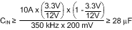
If the system design requires a certain minimum value of peak-to-peak input ripple voltage (ΔVIN) to be maintained then Equation 13 may be used.
If ΔVIN is 200 mV or 1.66% of VIN for a 12-V input to 3.3-V output application and fSW = 350 kHz then:
Additional bulk capacitance with higher ESR can be required to damp any resonant effects of the input capacitance and parasitic inductance of the incoming supply lines. The LMZ12010 typical applications schematic and evaluation board include a 150-μF 50-V aluminum capacitor for this function. There are many situations where this capacitor is not necessary.