ZHCSL09C April   2020  – December 2020 LM7480-Q1

PRODUCTION DATA  

  1. 特性
  2. 应用
  3. 说明
  4. Revision History
  5. Device Comparison Table
  6. Pin Configuration and Functions
  7. Specifications
    1. 7.1 Absolute Maximum Ratings
    2. 7.2 ESD Ratings
    3. 7.3 Recommended Operating Conditions
    4. 7.4 Thermal Information
    5. 7.5 Electrical Characteristics
    6. 7.6 Switching Characteristics
    7. 7.7 Typical Characteristics
  8. Parameter Measurement Information
  9. Detailed Description
    1. 9.1 Overview
    2. 9.2 Functional Block Diagram
    3. 9.3 Feature Description
      1. 9.3.1 Charge Pump
      2. 9.3.2 Dual Gate Control (DGATE, HGATE)
        1. 9.3.2.1 Reverse Battery Protection (A, C, DGATE)
        2. 9.3.2.2 Load Disconnect Switch Control (HGATE, OUT)
      3. 9.3.3 Overvoltage Protection and Battery Voltage Sensing (VSNS, SW, OV)
      4. 9.3.4 Low Iq Shutdown and Under Voltage Lockout (EN/UVLO)
    4. 9.4 Device Functional Modes
    5. 9.5 Application Examples
      1. 9.5.1 Redundant Supply OR-ing with Inrush Current Limiting, Overvoltage Protection and ON/OFF Control
      2. 9.5.2 Ideal Diode with Unsuppressed Load Dump Protection
  10. 10Applications and Implementation
    1. 10.1 Application Information
    2. 10.2 Typical 12-V Reverse Battery Protection Application
      1. 10.2.1 Design Requirements for 12-V Battery Protection
      2. 10.2.2 Automotive Reverse Battery Protection
        1. 10.2.2.1 Input Transient Protection: ISO 7637-2 Pulse 1
        2. 10.2.2.2 AC Super Imposed Input Rectification: ISO 16750-2 and LV124 E-06
        3. 10.2.2.3 Input Micro-Short Protection: LV124 E-10
      3. 10.2.3 Detailed Design Procedure
        1. 10.2.3.1 Design Considerations
        2. 10.2.3.2 Charge Pump Capacitance VCAP
        3. 10.2.3.3 Input and Output Capacitance
        4. 10.2.3.4 Hold-Up Capacitance
        5. 10.2.3.5 Overvoltage Protection and Battery Monitor
      4. 10.2.4 MOSFET Selection: Blocking MOSFET Q1
      5. 10.2.5 MOSFET Selection: Hot-Swap MOSFET Q2
      6. 10.2.6 TVS Selection
      7. 10.2.7 Application Curves
    3. 10.3 200-V Unsuppressed Load Dump Protection Application
      1. 10.3.1 Design Requirements for 200-V Unsuppressed Load Dump Protection
      2. 10.3.2 Design Procedure
        1. 10.3.2.1 Charge Pump Capacitance VCAP
        2. 10.3.2.2 Input and output capacitance
        3. 10.3.2.3 VS Capacitance, Resistor and Zener Clamp
        4. 10.3.2.4 Overvoltage Protection and Output Clamp
        5. 10.3.2.5 MOSFET Q1 Selection
        6. 10.3.2.6 Input TVS Selection
        7. 10.3.2.7 MOSFET Q2 Selection
      3. 10.3.3 Application Curves
    4. 10.4 Do's and Don'ts
  11. 11Power Supply Recommendations
    1. 11.1 Transient Protection
    2. 11.2 TVS Selection for 12-V Battery Systems
    3. 11.3 TVS Selection for 24-V Battery Systems
  12. 12Layout
    1. 12.1 Layout Guidelines
    2. 12.2 Layout Example
  13. 13Device and Documentation Support
    1. 13.1 Receiving Notification of Documentation Updates
    2. 13.2 Support Resources
    3. 13.3 Trademarks
    4. 13.4 Electrostatic Discharge Caution
    5. 13.5 Glossary
  14. 14Mechanical, Packaging, and Orderable Information

封装选项

机械数据 (封装 | 引脚)
散热焊盘机械数据 (封装 | 引脚)
订购信息

Application Curves

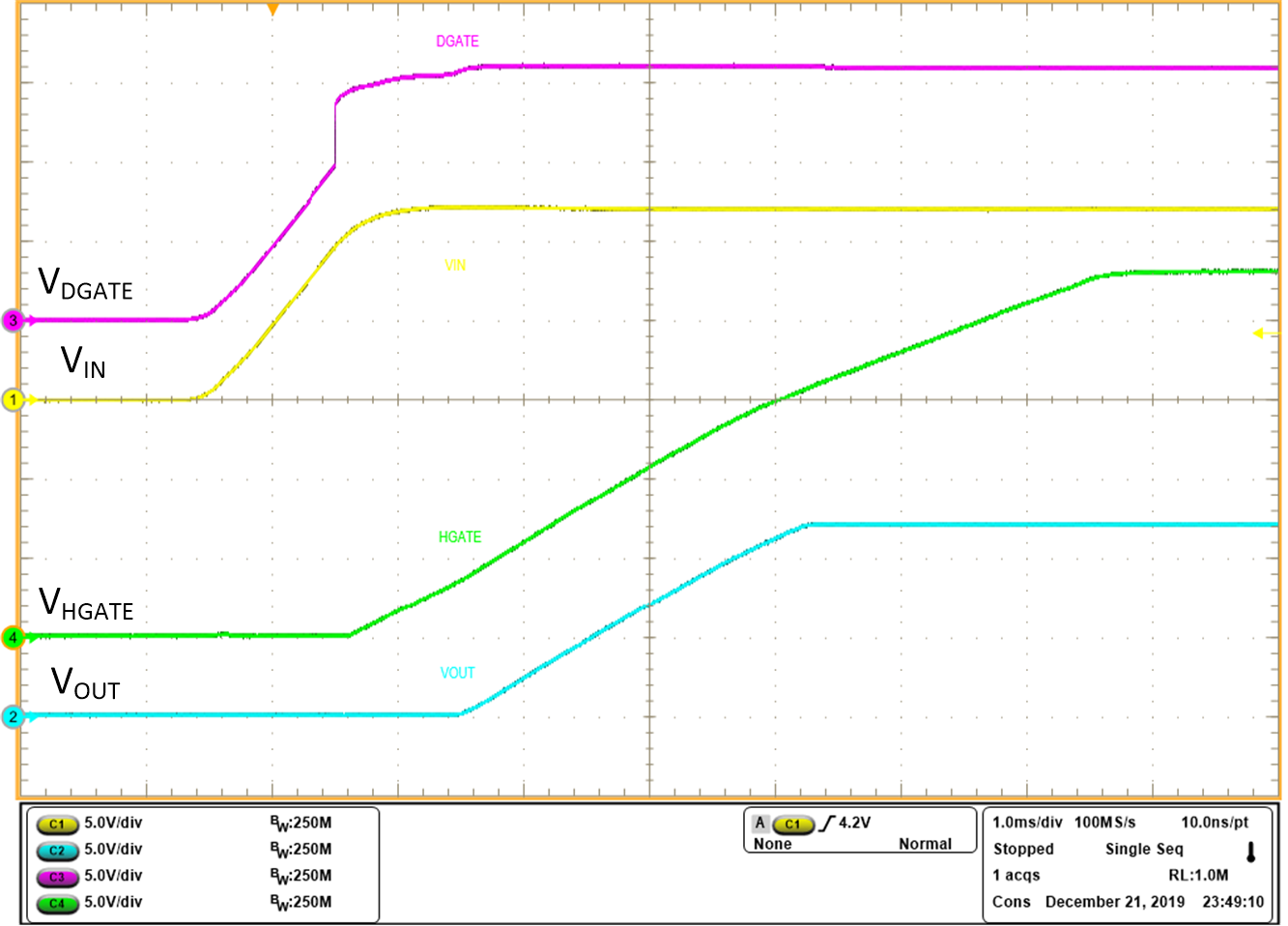
GUID-C24AF833-58DB-4296-99B4-8E708E81548A-low.pngFigure 10-7 Startup 12 V with EN Pulled to VIN
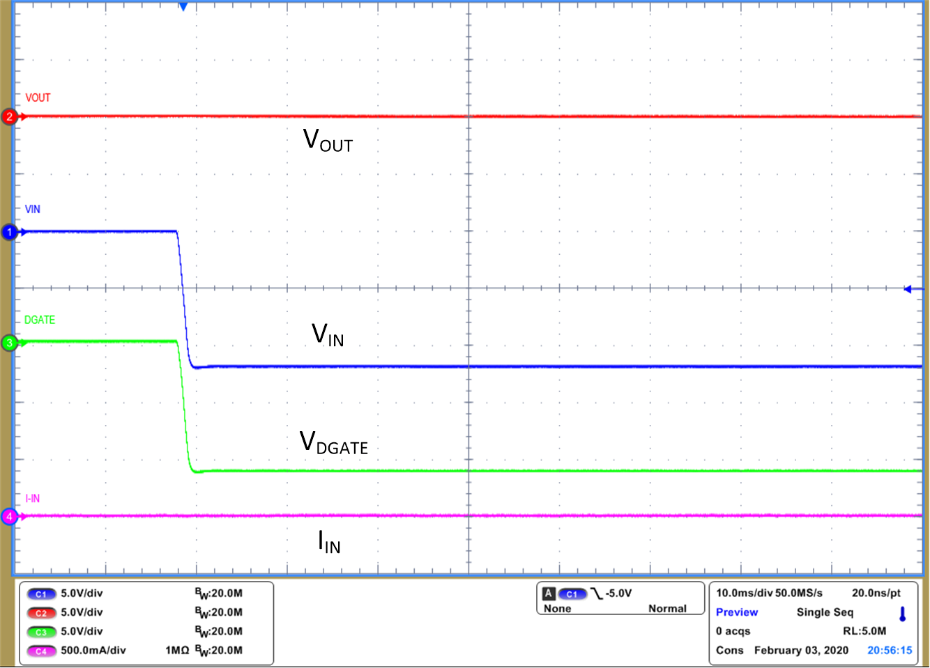
GUID-4CFC2521-FC71-4FF1-B5F0-E368996A22A9-low.pngFigure 10-9 Reverse Input Voltage –14 V
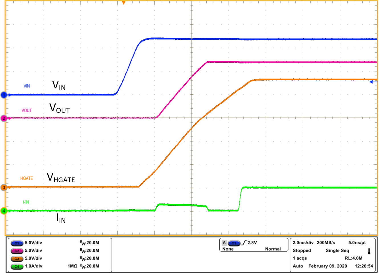
GUID-29250E21-5FE6-403A-B1B4-508FE9A651B2-low.pngFigure 10-11 Inrush Current with no Load at Output
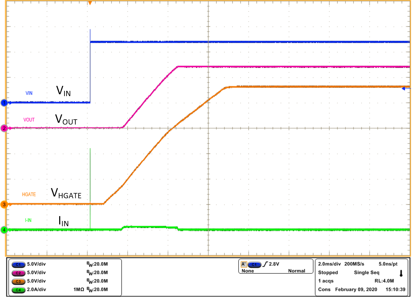
GUID-05C20542-7629-4033-ACA9-EFBEEC05FF18-low.pngFigure 10-13 Hot-Plug into 12 V
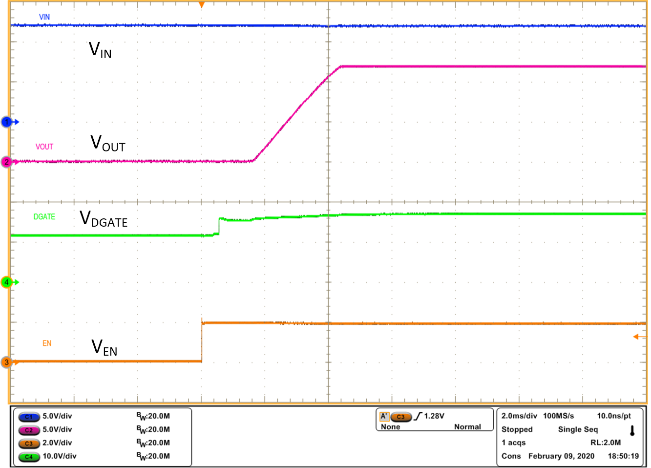
GUID-5085C78B-7FCB-4FDB-8CC8-2AF5316BA318-low.pngFigure 10-15 DGATE Turn ON with Enable
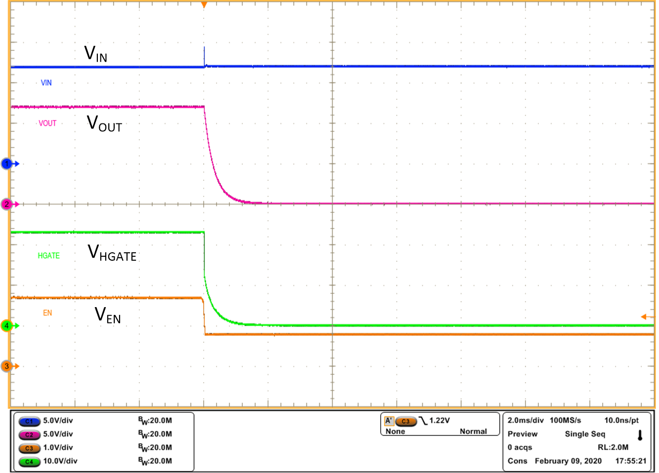
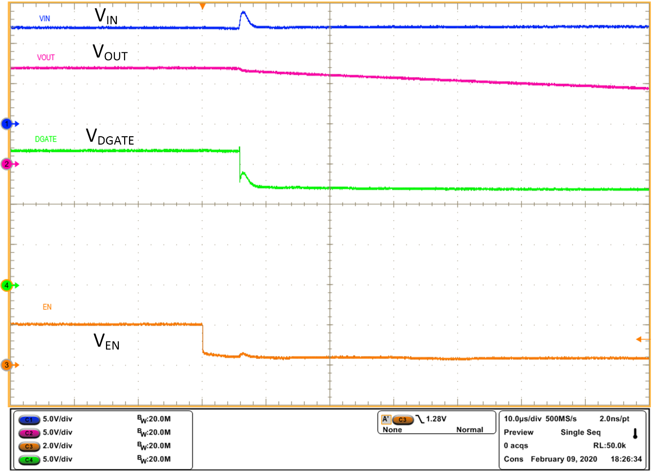
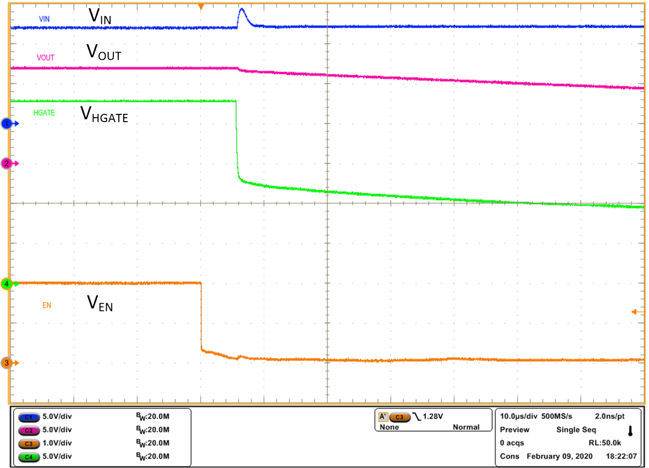
GUID-77903FD9-1417-4B94-8395-90507D86B009-low.pngFigure 10-17 Turn OFF with Enable Control
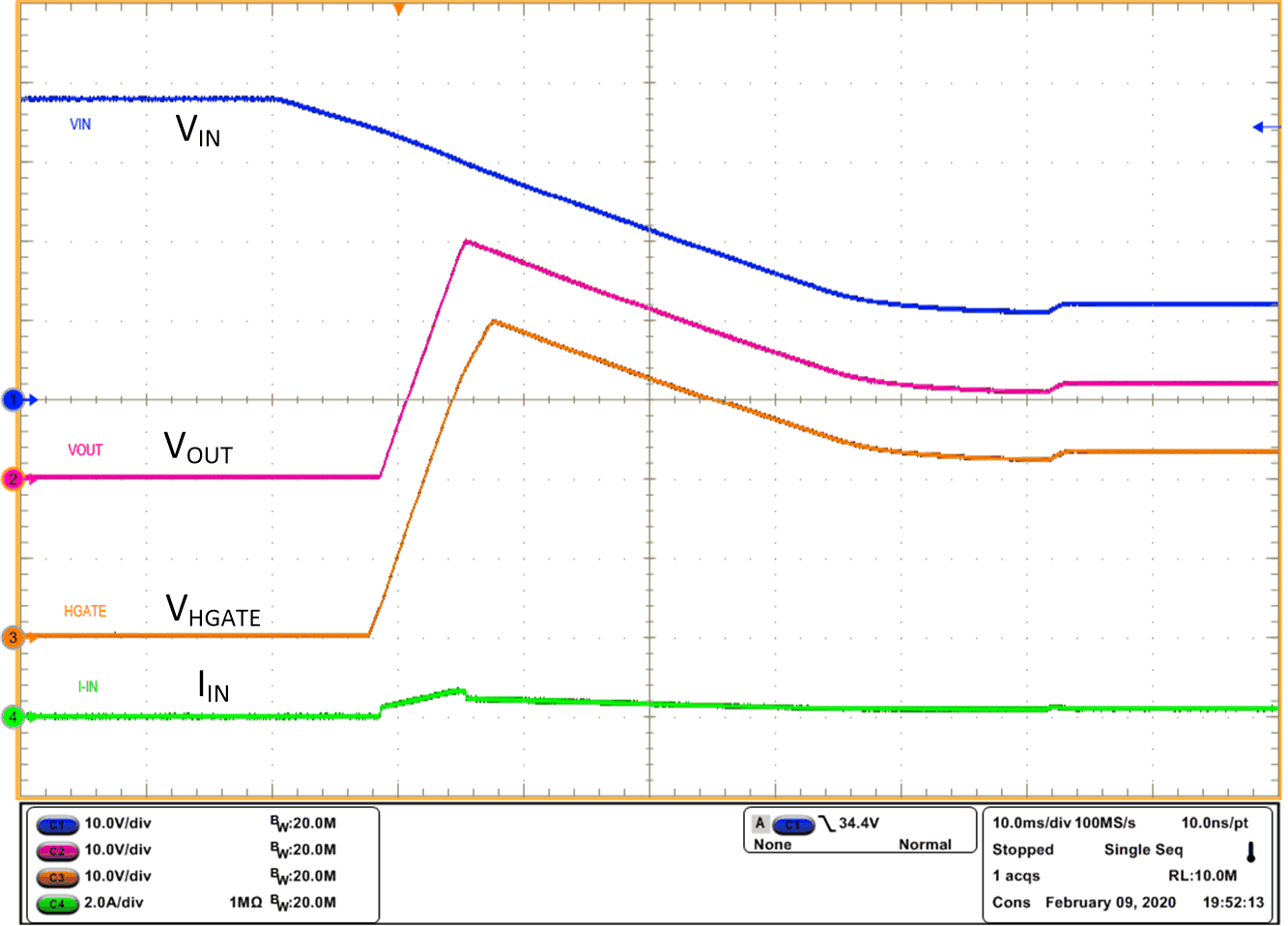
GUID-A1DD4172-97C0-4217-80F6-EAFA55E7995F-low.gifFigure 10-19 Overvoltage Recovery
GUID-46CCC45A-4F85-4A58-83A9-896504952547-low.pngFigure 10-21 Turn OFF Delay - DGATE
GUID-893271B5-DD6E-479B-97C1-05A51C973275-low.pngFigure 10-23 Load Transient 100 mA to 5 A
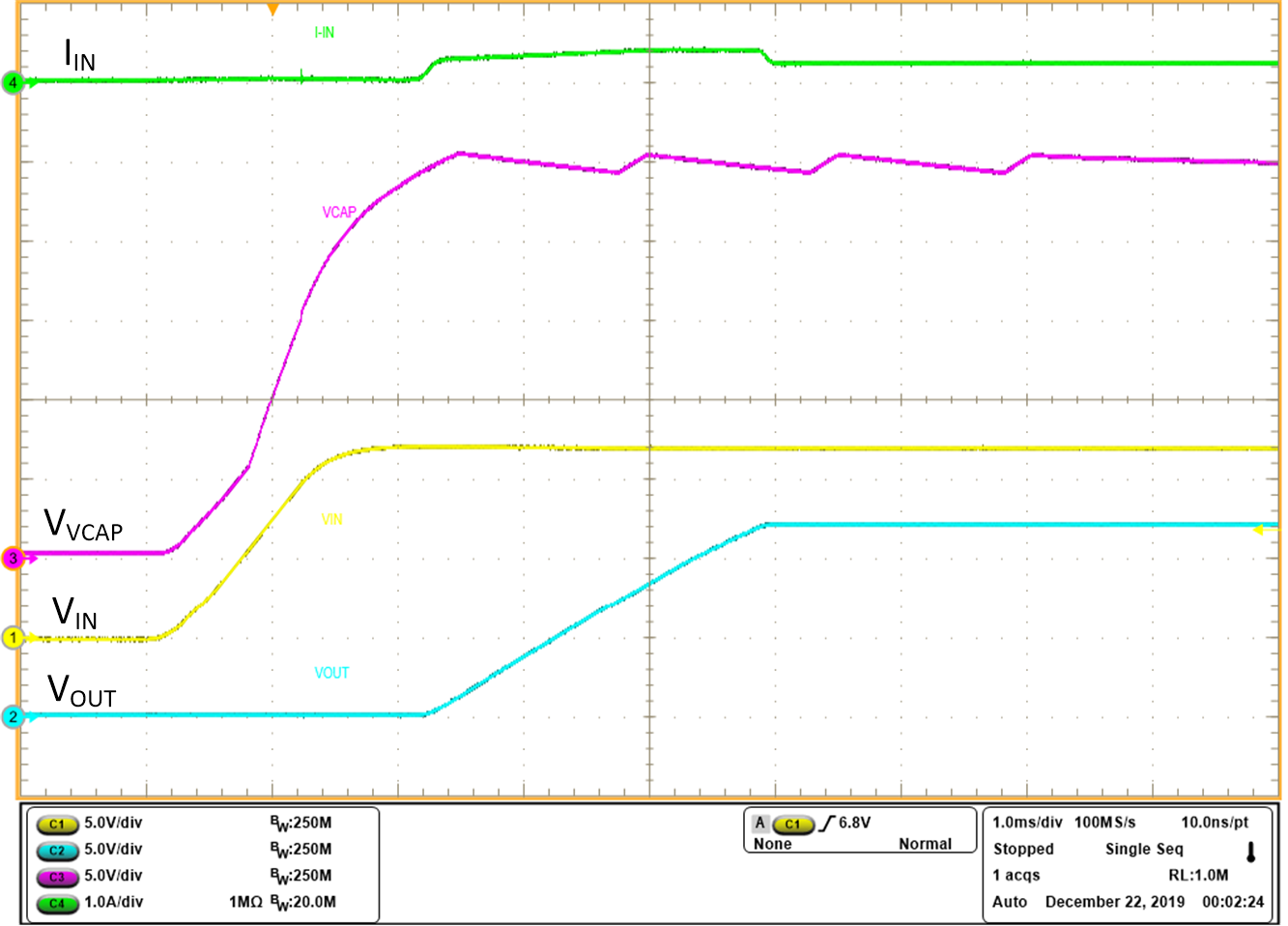
GUID-8036EE2C-A2CE-48DD-83C7-CB071C308506-low.pngFigure 10-8 Startup 12 V showing Charge Pump VCAP
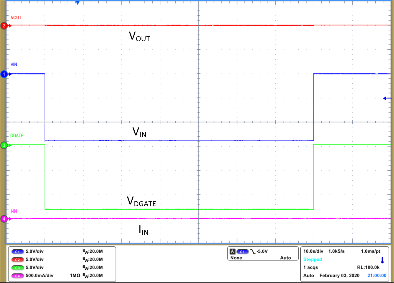
GUID-A04DD10D-DE98-460D-A096-8B659F44342A-low.pngFigure 10-10 Reverse Input Voltage –14 V for 60 s
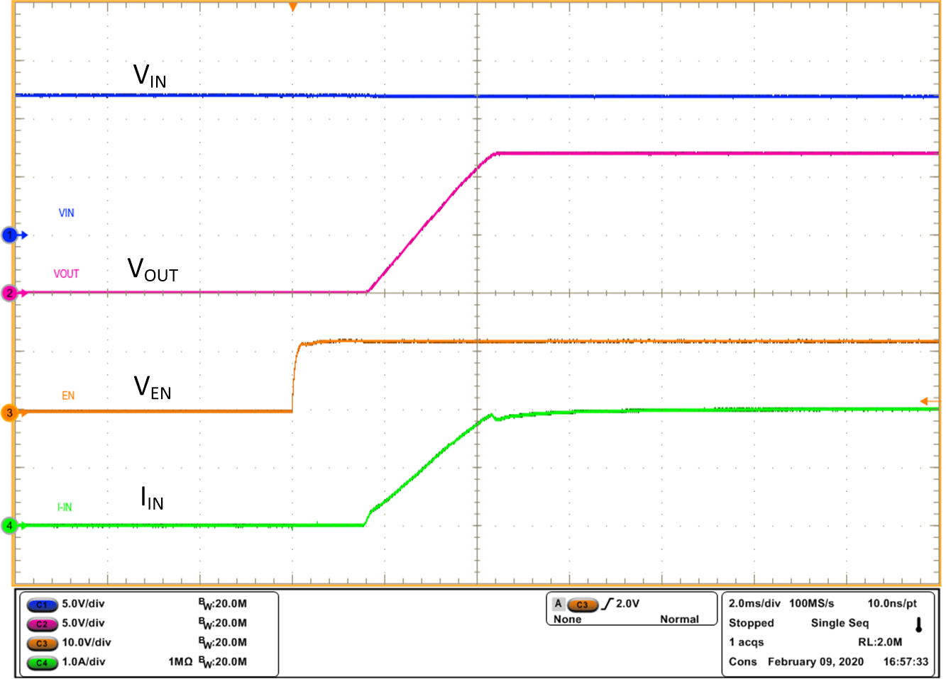
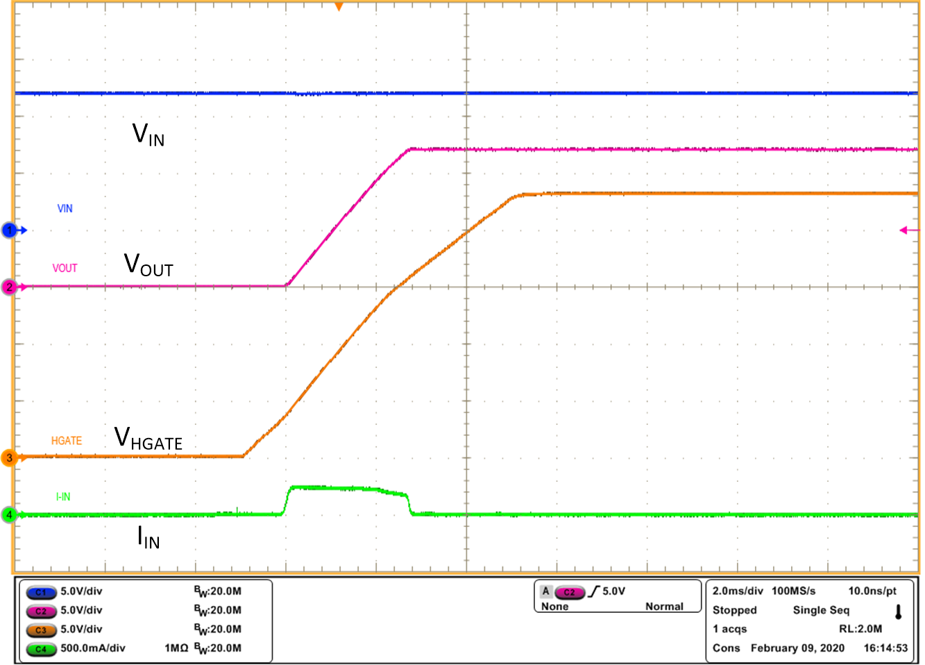
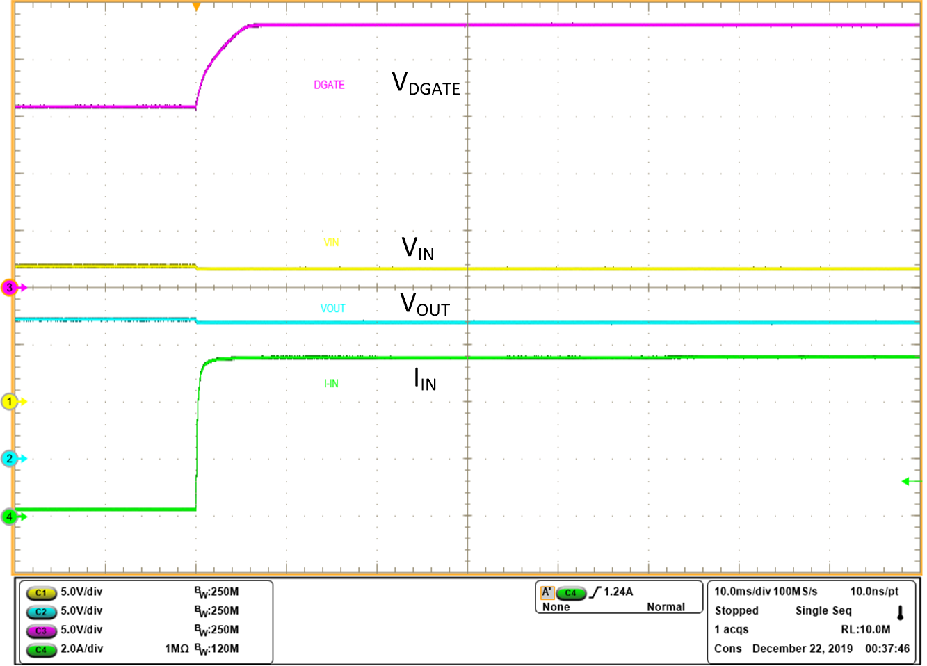
GUID-68740AE8-6F47-471C-9165-8B4E20CEE5BF-low.pngFigure 10-12 Inrush Current with 60-Ω Load
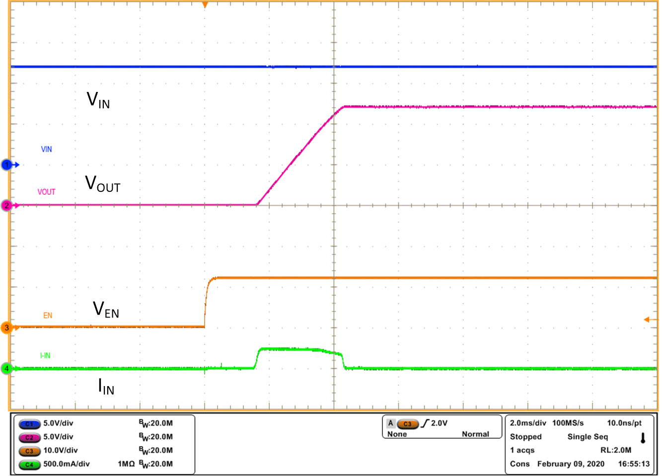
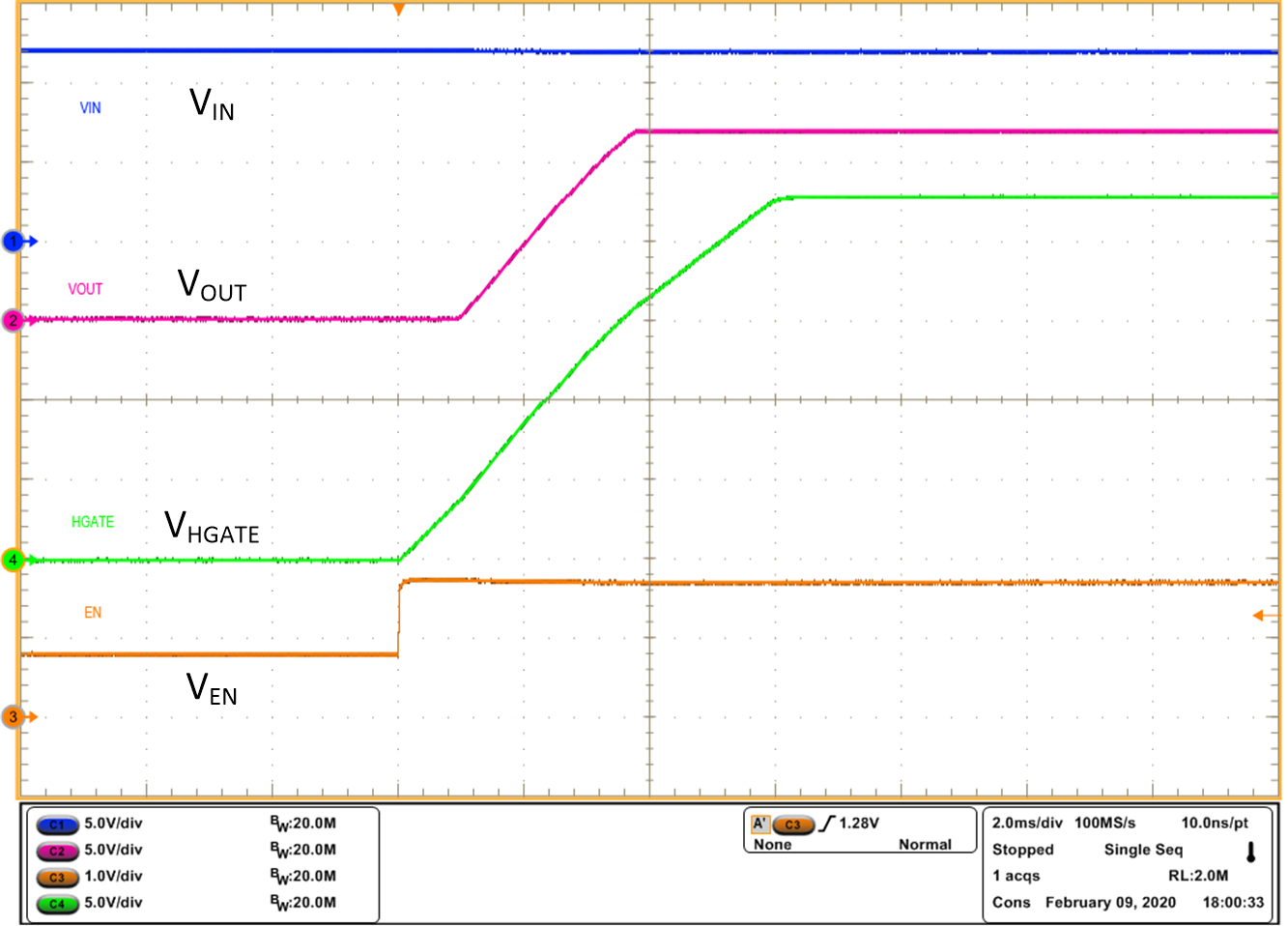
GUID-C40078C3-59D6-4D35-AB9D-E9F1CDE6D714-low.pngFigure 10-14 Output Turn ON with Enable
GUID-50155E25-7FA4-41DF-9D6B-970F757BA354-low.pngFigure 10-16 Turn ON with VCAP ON - EN rising from 0.8 V
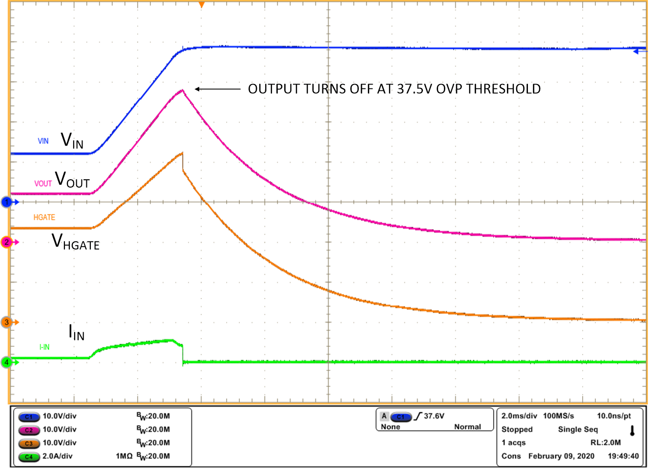
GUID-DB08D41E-ABDA-435D-AA01-5B0541482CD4-low.pngFigure 10-18 Overvoltage Protection
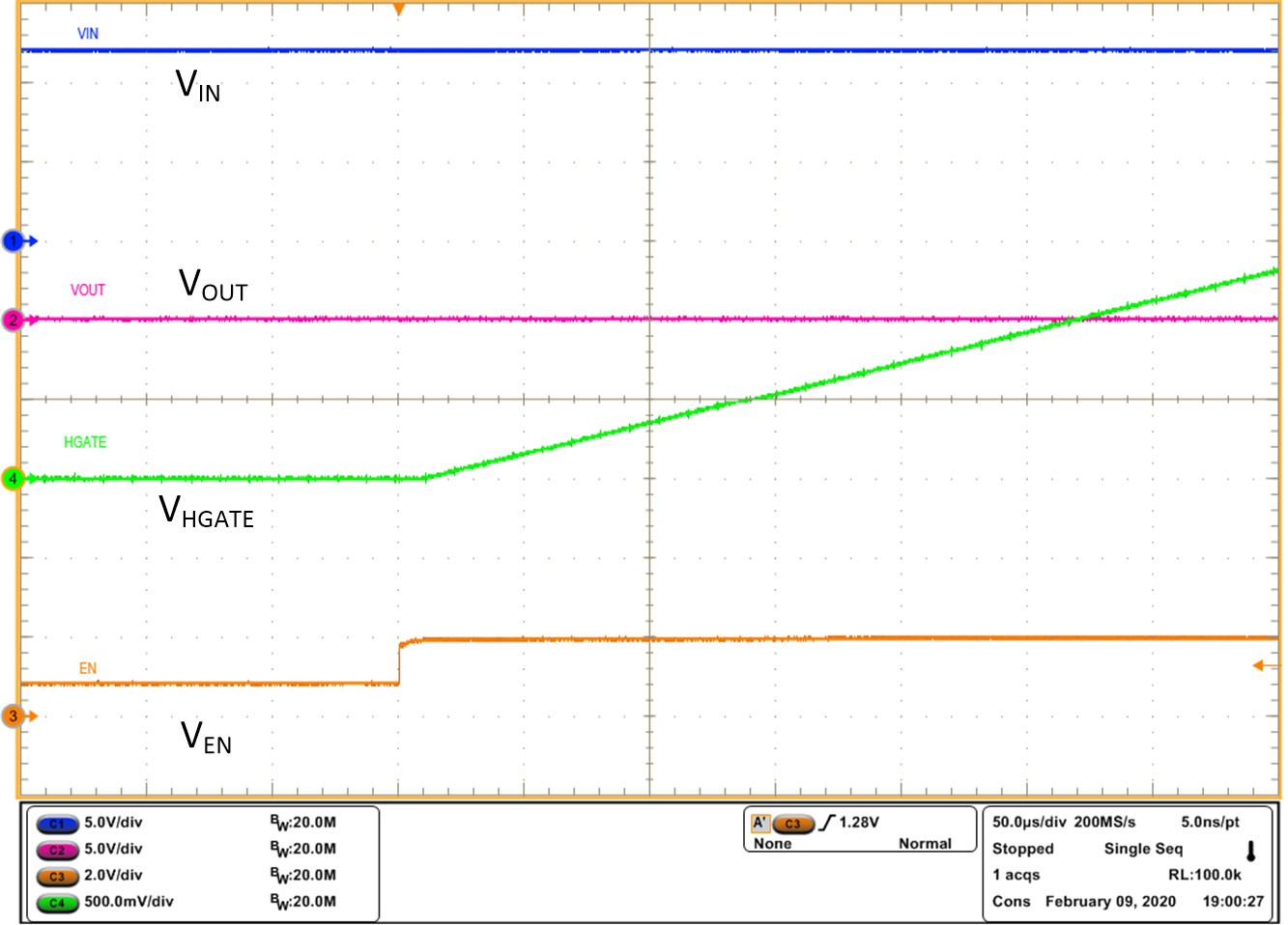
GUID-59936D00-7574-4BB0-AFE9-06407931F3CF-low.pngFigure 10-20 Turn ON delay - HGATE
GUID-99F70E05-D33F-46B6-92FA-1AE18835901F-low.pngFigure 10-22 Turn OFF Delay - HGATE
GUID-CECC5800-FC00-41E9-BB78-5FD73AAF5DE7-low.pngFigure 10-24 Startup 1-A Load 1 ms After Output Powers Up