ZHCSL09C April   2020  – December 2020 LM7480-Q1

PRODUCTION DATA  

  1. 特性
  2. 应用
  3. 说明
  4. Revision History
  5. Device Comparison Table
  6. Pin Configuration and Functions
  7. Specifications
    1. 7.1 Absolute Maximum Ratings
    2. 7.2 ESD Ratings
    3. 7.3 Recommended Operating Conditions
    4. 7.4 Thermal Information
    5. 7.5 Electrical Characteristics
    6. 7.6 Switching Characteristics
    7. 7.7 Typical Characteristics
  8. Parameter Measurement Information
  9. Detailed Description
    1. 9.1 Overview
    2. 9.2 Functional Block Diagram
    3. 9.3 Feature Description
      1. 9.3.1 Charge Pump
      2. 9.3.2 Dual Gate Control (DGATE, HGATE)
        1. 9.3.2.1 Reverse Battery Protection (A, C, DGATE)
        2. 9.3.2.2 Load Disconnect Switch Control (HGATE, OUT)
      3. 9.3.3 Overvoltage Protection and Battery Voltage Sensing (VSNS, SW, OV)
      4. 9.3.4 Low Iq Shutdown and Under Voltage Lockout (EN/UVLO)
    4. 9.4 Device Functional Modes
    5. 9.5 Application Examples
      1. 9.5.1 Redundant Supply OR-ing with Inrush Current Limiting, Overvoltage Protection and ON/OFF Control
      2. 9.5.2 Ideal Diode with Unsuppressed Load Dump Protection
  10. 10Applications and Implementation
    1. 10.1 Application Information
    2. 10.2 Typical 12-V Reverse Battery Protection Application
      1. 10.2.1 Design Requirements for 12-V Battery Protection
      2. 10.2.2 Automotive Reverse Battery Protection
        1. 10.2.2.1 Input Transient Protection: ISO 7637-2 Pulse 1
        2. 10.2.2.2 AC Super Imposed Input Rectification: ISO 16750-2 and LV124 E-06
        3. 10.2.2.3 Input Micro-Short Protection: LV124 E-10
      3. 10.2.3 Detailed Design Procedure
        1. 10.2.3.1 Design Considerations
        2. 10.2.3.2 Charge Pump Capacitance VCAP
        3. 10.2.3.3 Input and Output Capacitance
        4. 10.2.3.4 Hold-Up Capacitance
        5. 10.2.3.5 Overvoltage Protection and Battery Monitor
      4. 10.2.4 MOSFET Selection: Blocking MOSFET Q1
      5. 10.2.5 MOSFET Selection: Hot-Swap MOSFET Q2
      6. 10.2.6 TVS Selection
      7. 10.2.7 Application Curves
    3. 10.3 200-V Unsuppressed Load Dump Protection Application
      1. 10.3.1 Design Requirements for 200-V Unsuppressed Load Dump Protection
      2. 10.3.2 Design Procedure
        1. 10.3.2.1 Charge Pump Capacitance VCAP
        2. 10.3.2.2 Input and output capacitance
        3. 10.3.2.3 VS Capacitance, Resistor and Zener Clamp
        4. 10.3.2.4 Overvoltage Protection and Output Clamp
        5. 10.3.2.5 MOSFET Q1 Selection
        6. 10.3.2.6 Input TVS Selection
        7. 10.3.2.7 MOSFET Q2 Selection
      3. 10.3.3 Application Curves
    4. 10.4 Do's and Don'ts
  11. 11Power Supply Recommendations
    1. 11.1 Transient Protection
    2. 11.2 TVS Selection for 12-V Battery Systems
    3. 11.3 TVS Selection for 24-V Battery Systems
  12. 12Layout
    1. 12.1 Layout Guidelines
    2. 12.2 Layout Example
  13. 13Device and Documentation Support
    1. 13.1 Receiving Notification of Documentation Updates
    2. 13.2 Support Resources
    3. 13.3 Trademarks
    4. 13.4 Electrostatic Discharge Caution
    5. 13.5 Glossary
  14. 14Mechanical, Packaging, and Orderable Information

封装选项

机械数据 (封装 | 引脚)
散热焊盘机械数据 (封装 | 引脚)
订购信息

Charge Pump

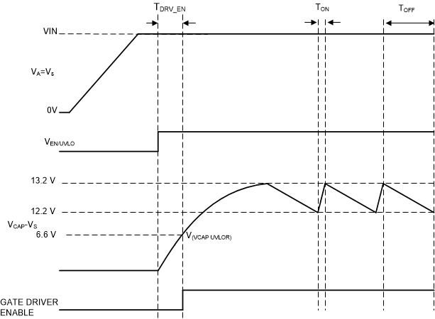
The charge pump supplies the voltage necessary to drive the external N-channel MOSFET. An external charge pump capacitor is placed between CAP and VS pins to provide energy to turn on the external MOSFET. In order for the charge pump to supply current to the external capacitor, the EN/UVLO pin voltage must be above the specified input high threshold, V(ENR). When enabled the charge pump sources a charging current of 2.7-mA typical. If EN/UVLO pin is pulled low, then the charge pump remains disabled. To ensure that the external MOSFET can be driven above its specified threshold voltage, the CAP to VS voltage must be above the undervoltage lockout threshold, typically 6.6 V, before the internal gate driver is enabled. Use Equation 1 to calculate the initial gate driver enable delay.

Equation 1. GUID-20201006-CA0I-JKHW-69VJ-TT0KRDQTQ5HB-low.gif

where

  • C(CAP) is the charge pump capacitance connected across VS and CAP pins
  • V(CAP_UVLOR) = 6.6 V (typical)

To remove any chatter on the gate drive approximately 1 V of hysteresis is added to the VCAP undervoltage lockout. The charge pump remains enabled until the CAP to VS voltage reaches 13.2 V, typically, at which point the charge pump is disabled decreasing the current draw on the VS pin. The charge pump remains disabled until the CAP to VS voltage is below to 12.2 V typically at which point the charge pump is enabled. The voltage between CAP and VS continue to charge and discharge between 12.2 V and 13.2 V as shown in Figure 9-1. By enabling and disabling the charge pump, the operating quiescent current of the LM7480x-Q1 is reduced. When the charge pump is disabled it sinks 15 µA.
GUID-20201006-CA0I-2TTB-JHCB-SKTW1LJRH4VR-low.gifFigure 9-1 Charge Pump Operation