ZHCSL09C April   2020  – December 2020 LM7480-Q1

PRODUCTION DATA  

  1. 特性
  2. 应用
  3. 说明
  4. Revision History
  5. Device Comparison Table
  6. Pin Configuration and Functions
  7. Specifications
    1. 7.1 Absolute Maximum Ratings
    2. 7.2 ESD Ratings
    3. 7.3 Recommended Operating Conditions
    4. 7.4 Thermal Information
    5. 7.5 Electrical Characteristics
    6. 7.6 Switching Characteristics
    7. 7.7 Typical Characteristics
  8. Parameter Measurement Information
  9. Detailed Description
    1. 9.1 Overview
    2. 9.2 Functional Block Diagram
    3. 9.3 Feature Description
      1. 9.3.1 Charge Pump
      2. 9.3.2 Dual Gate Control (DGATE, HGATE)
        1. 9.3.2.1 Reverse Battery Protection (A, C, DGATE)
        2. 9.3.2.2 Load Disconnect Switch Control (HGATE, OUT)
      3. 9.3.3 Overvoltage Protection and Battery Voltage Sensing (VSNS, SW, OV)
      4. 9.3.4 Low Iq Shutdown and Under Voltage Lockout (EN/UVLO)
    4. 9.4 Device Functional Modes
    5. 9.5 Application Examples
      1. 9.5.1 Redundant Supply OR-ing with Inrush Current Limiting, Overvoltage Protection and ON/OFF Control
      2. 9.5.2 Ideal Diode with Unsuppressed Load Dump Protection
  10. 10Applications and Implementation
    1. 10.1 Application Information
    2. 10.2 Typical 12-V Reverse Battery Protection Application
      1. 10.2.1 Design Requirements for 12-V Battery Protection
      2. 10.2.2 Automotive Reverse Battery Protection
        1. 10.2.2.1 Input Transient Protection: ISO 7637-2 Pulse 1
        2. 10.2.2.2 AC Super Imposed Input Rectification: ISO 16750-2 and LV124 E-06
        3. 10.2.2.3 Input Micro-Short Protection: LV124 E-10
      3. 10.2.3 Detailed Design Procedure
        1. 10.2.3.1 Design Considerations
        2. 10.2.3.2 Charge Pump Capacitance VCAP
        3. 10.2.3.3 Input and Output Capacitance
        4. 10.2.3.4 Hold-Up Capacitance
        5. 10.2.3.5 Overvoltage Protection and Battery Monitor
      4. 10.2.4 MOSFET Selection: Blocking MOSFET Q1
      5. 10.2.5 MOSFET Selection: Hot-Swap MOSFET Q2
      6. 10.2.6 TVS Selection
      7. 10.2.7 Application Curves
    3. 10.3 200-V Unsuppressed Load Dump Protection Application
      1. 10.3.1 Design Requirements for 200-V Unsuppressed Load Dump Protection
      2. 10.3.2 Design Procedure
        1. 10.3.2.1 Charge Pump Capacitance VCAP
        2. 10.3.2.2 Input and output capacitance
        3. 10.3.2.3 VS Capacitance, Resistor and Zener Clamp
        4. 10.3.2.4 Overvoltage Protection and Output Clamp
        5. 10.3.2.5 MOSFET Q1 Selection
        6. 10.3.2.6 Input TVS Selection
        7. 10.3.2.7 MOSFET Q2 Selection
      3. 10.3.3 Application Curves
    4. 10.4 Do's and Don'ts
  11. 11Power Supply Recommendations
    1. 11.1 Transient Protection
    2. 11.2 TVS Selection for 12-V Battery Systems
    3. 11.3 TVS Selection for 24-V Battery Systems
  12. 12Layout
    1. 12.1 Layout Guidelines
    2. 12.2 Layout Example
  13. 13Device and Documentation Support
    1. 13.1 Receiving Notification of Documentation Updates
    2. 13.2 Support Resources
    3. 13.3 Trademarks
    4. 13.4 Electrostatic Discharge Caution
    5. 13.5 Glossary
  14. 14Mechanical, Packaging, and Orderable Information

封装选项

机械数据 (封装 | 引脚)
散热焊盘机械数据 (封装 | 引脚)
订购信息

Ideal Diode with Unsuppressed Load Dump Protection

An extended overvoltage protection support above 65 V can be achieved by configuring the device with external back to back MOSFETs in common source topology as shown in Figure 9-6. Place a resistor R1 and a zener clamp across VS pin to GND to limit the voltage below 65 V. The load gets protected from overvoltages transients like un-suppressed load dumps with the help of overvoltage protection feature. Use R2 and R3 for setting the overvoltage protection threshold. When voltage at OV pin exceeds the set OV threshold then the HGATE turns OFF. This results in power path disconnection between input and output.
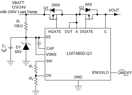
GUID-7676E02F-DC2B-4723-87F2-4D9FB70E4CAA-low.gif Figure 9-6 Ideal Diode with 200-V Unsupressed Load Dump Protection