ZHCSOA2A July 2020 – July 2021 LM63610-Q1
PRODUCTION DATA
- 1 特性
- 2 应用
- 3 说明
- 4 Revision History
- 5 Device Comparison Table
- 6 Pin Configuration and Functions
- 7 Specifications
- 8 Detailed Description
- 9 Application and Implementation
- 10Power Supply Recommendations
- 11Layout
- 12Device and Documentation Support
- 13Mechanical, Packaging, and Orderable Information
封装选项
机械数据 (封装 | 引脚)
散热焊盘机械数据 (封装 | 引脚)
订购信息
8.3.5 RESET Flag Output
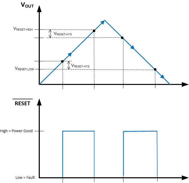
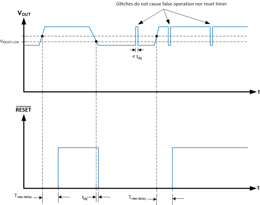
The RESET flag function (RESET output pin) of the LM63610-Q1 devices can be used to reset a system microprocessor whenever the output voltage is out of regulation. This open-drain output goes low under fault conditions, such as current limit and thermal shutdown, as well as during normal start-up. A glitch filter prevents false flag operation for short excursions of the output voltage, such as during line and load transients. Output voltage excursions lasting less than tdg do not trip the RESET flag. Once the FB voltage has returned to the regulation value and after a delay of trise-delay, the RESET flag goes high. RESET operation can best be understood by reference to Figure 8-3 and Figure 8-4.
The RESET output consists of an open-drain NMOS, requiring an external pullup resistor to a suitable logic supply. It can also be pulled up to either VCC or VOUT through an appropriate resistor, as desired. Values of pullup resistor in the range of 10 kΩ to 100 kΩ are reasonable. If this function is not needed, the RESET pin can be left floating. When EN is pulled low, the flag output is also forced low. With EN low, RESET remains valid as long as the input voltage is ≥ 1.2 V (typical). Limit the current into the RESET flag pin to about 5 mA D.C. The maximum current is internally limited to about 50 mA when the device is enabled and about 65 mA when the device is disabled. The internal current limit protects the device from any transient currents that can occur when discharging a filter capacitor connected to this output.
 Figure 8-3 Static
RESET Operation
 Figure 8-4 RESET Timing Behavior