SNVS397F September   2005  – December 2025 LM5005

PRODUCTION DATA  

  1.   1
  2. Features
  3. Applications
  4. Description
  5. Pin Configuration and Functions
  6. Specifications
    1. 5.1 Absolute Maximum Ratings
    2. 5.2 ESD Ratings
    3. 5.3 Recommended Operating Conditions
    4. 5.4 Thermal Information
    5. 5.5 Electrical Characteristics
    6. 5.6 Switching Characteristics
    7. 5.7 Typical Characteristics
  7. Detailed Description
    1. 6.1 Overview
    2. 6.2 Functional Block Diagram
    3. 6.3 Feature Description
      1. 6.3.1 High-Voltage Start-Up Regulator
      2. 6.3.2 Shutdown and Standby
      3. 6.3.3 Oscillator and Synchronization Capability
      4. 6.3.4 Error Amplifier and PWM Comparator
      5. 6.3.5 RAMP Generator
      6. 6.3.6 Current Limit
      7. 6.3.7 Soft-Start Capability
      8. 6.3.8 MOSFET Gate Driver
    4. 6.4 Device Functional Modes
      1. 6.4.1 Shutdown Mode
      2. 6.4.2 Standby Mode
      3. 6.4.3 Light-Load Operation
      4. 6.4.4 Thermal Shutdown Protection
  8. Application and Implementation
    1. 7.1 Application Information
      1. 7.1.1 Reducing Bias Power Dissipation
      2. 7.1.2 Input Voltage UVLO Protection
    2. 7.2 Typical Application
      1. 7.2.1 Design Requirements
      2. 7.2.2 Detailed Design Procedure
        1. 7.2.2.1  Custom Design With WEBENCH® Tools
        2. 7.2.2.2  Frequency Set Resistor (RT)
        3. 7.2.2.3  Inductor (LF)
        4. 7.2.2.4  Ramp Capacitor (CRAMP)
        5. 7.2.2.5  Output Capacitors (COUT)
        6. 7.2.2.6  Schottky Diode (DF)
        7. 7.2.2.7  Input Capacitors (CIN)
        8. 7.2.2.8  VCC Capacitor (CVCC)
        9. 7.2.2.9  Bootstrap Capacitor (CBST)
        10. 7.2.2.10 Soft Start Capacitor (CSS)
        11. 7.2.2.11 Feedback Resistors (RFB1 and RFB2)
        12. 7.2.2.12 RC Snubber (RS and CS)
        13. 7.2.2.13 Compensation Components (RC1, CC1, CC2)
        14. 7.2.2.14 Bill of Materials
      3. 7.2.3 Application Curves
    3. 7.3 Power Supply Recommendations
    4. 7.4 Layout
      1. 7.4.1 Layout Guidelines
        1. 7.4.1.1 PCB Layout for EMI Reduction
        2. 7.4.1.2 Thermal Design
        3. 7.4.1.3 Ground Plane Design
      2. 7.4.2 Layout Example
  9. Device and Documentation Support
    1. 8.1 Third-Party Products Disclaimer
    2. 8.2 Device Support
      1. 8.2.1 Development Support
        1. 8.2.1.1 Custom Design With WEBENCH® Tools
    3. 8.3 Documentation Support
      1. 8.3.1 Related Documentation
        1. 8.3.1.1 PCB Layout Resources
        2. 8.3.1.2 Thermal Design Resources
    4. 8.4 Receiving Notification of Documentation Updates
    5. 8.5 Support Resources
    6. 8.6 Trademarks
    7. 8.7 Electrostatic Discharge Caution
    8. 8.8 Glossary
  10. Revision History
  11. 10Mechanical, Packaging, and Orderable Information

封装选项

机械数据 (封装 | 引脚)
散热焊盘机械数据 (封装 | 引脚)
订购信息

Typical Characteristics

Unless otherwise specified, VIN = 48V and VOUT = 5V (see Typical Application for circuit designs).
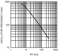
LM5005 Oscillator Frequency vs RT
Figure 5-1 Oscillator Frequency vs RT
LM5005 Oscillator Frequency vs Temperature
FOSC = 200kHz
Figure 5-2 Oscillator Frequency vs Temperature
LM5005 Soft-Start Current vs Temperature
Figure 5-3 Soft-Start Current vs Temperature
LM5005 VCC vs VIN
RL = 7kΩ
Figure 5-5 VCC vs VIN
LM5005 LM5005 Evaluation Board Efficiency vs IOUT and VINFigure 5-7 LM5005 Evaluation Board Efficiency vs IOUT and VIN
LM5005 VCC vs ICC
VIN = 12V
Figure 5-4 VCC vs ICC
LM5005 Error Amplifier Gain and Phase
AVCL = 101
Figure 5-6 Error Amplifier Gain and Phase