SNVS397F September 2005 – December 2025 LM5005
PRODUCTION DATA
- 1
- 1 Features
- 2 Applications
- 3 Description
- 4 Pin Configuration and Functions
- 5 Specifications
- 6 Detailed Description
-
7 Application and Implementation
- 7.1 Application Information
- 7.2
Typical Application
- 7.2.1 Design Requirements
- 7.2.2
Detailed Design Procedure
- 7.2.2.1 Custom Design With WEBENCH® Tools
- 7.2.2.2 Frequency Set Resistor (RT)
- 7.2.2.3 Inductor (LF)
- 7.2.2.4 Ramp Capacitor (CRAMP)
- 7.2.2.5 Output Capacitors (COUT)
- 7.2.2.6 Schottky Diode (DF)
- 7.2.2.7 Input Capacitors (CIN)
- 7.2.2.8 VCC Capacitor (CVCC)
- 7.2.2.9 Bootstrap Capacitor (CBST)
- 7.2.2.10 Soft Start Capacitor (CSS)
- 7.2.2.11 Feedback Resistors (RFB1 and RFB2)
- 7.2.2.12 RC Snubber (RS and CS)
- 7.2.2.13 Compensation Components (RC1, CC1, CC2)
- 7.2.2.14 Bill of Materials
- 7.2.3 Application Curves
- 7.3 Power Supply Recommendations
- 7.4 Layout
- 8 Device and Documentation Support
- 9 Revision History
- 10Mechanical, Packaging, and Orderable Information
7.2.2.13 Compensation Components (RC1, CC1, CC2)
These components configure the error amplifier gain characteristics to accomplish a stable overall loop gain. One advantage of current-mode control is the ability to close the loop with only two feedback components, RC1 and CC1. The overall loop gain is the product of the modulator gain and the error amplifier gain. The DC modulator gain of the LM5005 is calculated with Equation 17.
The dominant low-frequency pole of the modulator is determined by the load resistance, RLOAD, and the output capacitance, COUT. Calculate the corner frequency of this pole with Equation 18.
For RLOAD = 5Ω and COUT = 177 µF, then fp(MOD) = 180Hz
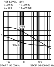
For this design example given RLOAD = 5Ω and COUT = 177 µF, Figure 7-6 shows the experimentally measured modulator gain versus frequency characteristic.
 Figure 7-6 PWM Modulator Gain and Phase Plot
Components RC1 and CC1 configure the error amplifier as a Type-II configuration, giving a pole at the origin and a zero at:
The error amplifier zero cancels the modulator pole leaving a single pole response at the crossover frequency of the loop gain. A single pole response at the crossover frequency yields a stable loop with 90° of phase margin.
For the design example, select a target loop bandwidth (crossover frequency) of 20kHz. Place the compensator zero frequency, fZ, an order of magnitude less than the target crossover frequency. This constrains the product of RC1 and CC1 for a desired compensation network zero frequency to be less than 2kHz. Increasing RC1 while proportionally decreasing CC1 increases the error amp gain. Conversely, decreasing RC1 while proportionally increasing CC1, decreases the error amp gain. Select RC1 of 49.9kΩ and CC1 of 10nF. These values configure the compensation network zero at 320Hz. The compensator gain at frequencies greater than fZ is RC1 / RFB1, which is approximately 20dB.
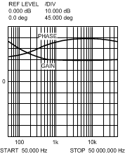
Figure 7-7 shows the compensator bode plot. The overall loop is predicted as the sum (in dB) of the modulator gain and the compensator gain as shown in Figure 7-8.
 Figure 7-7 Compensator Gain and Phase Plot
 Figure 7-8 Overall Loop Gain and Phase Plot
If a network analyzer is available, measure the modulator gain and configure the compensator gain for the desired loop transfer function. If a network analyzer is not available, design the compensation components of the error amplifier using the guidelines provided. Perform step-load transient tests to verify acceptable performance. The step load goal is minimum overshoot with a damped response. Add a capacitor CC2 to the compensation network to decrease noise susceptibility of the error amplifier. Verify that the value of CC2 is sufficiently small, because the addition of this capacitor adds a pole in the compensator transfer function. Verify that the pole is well beyond the loop crossover frequency. A good approximation of the location of the pole added by CC2 is Equation 21.
An alternative method to decrease the error amplifier noise susceptibility is to connect a capacitor from COMP to AGND. When using this method, establish that the capacitance of CC2 does not exceed 100pF.