SNVS397F September 2005 – December 2025 LM5005
PRODUCTION DATA
- 1
- 1 Features
- 2 Applications
- 3 Description
- 4 Pin Configuration and Functions
- 5 Specifications
- 6 Detailed Description
-
7 Application and Implementation
- 7.1 Application Information
- 7.2
Typical Application
- 7.2.1 Design Requirements
- 7.2.2
Detailed Design Procedure
- 7.2.2.1 Custom Design With WEBENCH® Tools
- 7.2.2.2 Frequency Set Resistor (RT)
- 7.2.2.3 Inductor (LF)
- 7.2.2.4 Ramp Capacitor (CRAMP)
- 7.2.2.5 Output Capacitors (COUT)
- 7.2.2.6 Schottky Diode (DF)
- 7.2.2.7 Input Capacitors (CIN)
- 7.2.2.8 VCC Capacitor (CVCC)
- 7.2.2.9 Bootstrap Capacitor (CBST)
- 7.2.2.10 Soft Start Capacitor (CSS)
- 7.2.2.11 Feedback Resistors (RFB1 and RFB2)
- 7.2.2.12 RC Snubber (RS and CS)
- 7.2.2.13 Compensation Components (RC1, CC1, CC2)
- 7.2.2.14 Bill of Materials
- 7.2.3 Application Curves
- 7.3 Power Supply Recommendations
- 7.4 Layout
- 8 Device and Documentation Support
- 9 Revision History
- 10Mechanical, Packaging, and Orderable Information
6.3.3 Oscillator and Synchronization Capability
The LM5005 oscillator frequency is set by a single external resistor designated RT connected between the RT and AGND pins. Place the RT resistor close to the LM5005 RT and AGND pins. Calculate the resistance of RT from Equation 1 to set a desired switching frequency, FSW.
Use the SYNC pin to synchronize the internal oscillator to an external clock. Verify that the external clock signal is of a higher frequency than the free-running frequency of the LM5005 set by the RT resistor. Figure 6-2 shows a clock circuit with an open-drain output and is the recommended interface to the SYNC pin. Establish that the clock pulse duration is greater than 15ns.
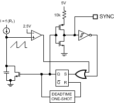
Simply connect the SYNC pins together to synchronize multiple LM5005 devices. In this configuration, all of the devices synchronize to the highest frequency device. The diagram in Figure 6-4 illustrates the SYNC input and output features of the LM5005. The internal oscillator circuit drives the SYNC pin with a strong pulldown and weak pullup inverter. When the SYNC pin is pulled low either by the internal oscillator or an external clock, the ramp cycle of the oscillator terminates and a new oscillator cycle begins. Thus, if the SYNC pins of several LM5005 IC connect together, the IC with the highest internal clock frequency pulls the connected SYNC pins low first and terminates the oscillator ramp cycles of the other ICs. The LM5005 with the highest programmed clock frequency serves as the controller and controls the switching frequency of all the devices with lower oscillator frequency.
 Figure 6-4 Simplified Oscillator Block Diagram and SYNC I/O Circuit