SNVSA38 November 2014 LM3281
PRODUCTION DATA.
- 1 Features
- 2 Applications
- 3 Description
- 4 Revision History
- 5 Pin Configuration and Functions
- 6 Specifications
- 7 Detailed Description
- 8 Application and Implementation
- 9 Power Supply Recommendations
- 10Layout
- 11Device and Documentation Support
- 12Mechanical, Packaging, and Orderable Information
6 Specifications
6.1 Absolute Maximum Ratings
over operating free-air temperature range (unless otherwise noted) (1)(2)| MIN | MAX | UNIT | ||
|---|---|---|---|---|
| VIN pin to GND pin voltage | –0.2 | 6 | V | |
| EN, FB, MODE, SW pins to GND pin voltage | –0.2 | VIN + 0.2 or 6 (whichever is smaller) |
||
| Junction temperature (TJ) | 150 | °C | ||
| Continuous power dissipation(3) | Internally limited | |||
| Maximum lead temperature (soldering) | 260 | °C | ||
(1) Stresses beyond those listed under Absolute Maximum Ratings may cause permanent damage to the device. These are stress ratings only, which do not imply functional operation of the device at these or any other conditions beyond those indicated under Recommended Operating Conditions. Exposure to absolute-maximum-rated conditions for extended periods may affect device reliability.
(2) If Military/Aerospace specified devices are required, please contact the Texas Instruments Sales Office/ Distributors for availability and specifications.
(3) Internal thermal shutdown circuitry protects the device from permanent damage. It engages at TJ = 150°C (typ.) and disengages at TJ = 125°C (typ.).
6.2 Handling Ratings
| MIN | MAX | UNIT | |||
|---|---|---|---|---|---|
| Tstg | Storage temperature range | –65 | 150 | °C | |
| V(ESD) | Electrostatic discharge | Human body model (HBM), per ANSI/ESDA/JEDEC JS-001, all pins(1) | –1000 | 1000 | V |
| Charged device model (CDM), per JEDEC specification JESD22-C101, all pins(2) | –250 | 250 | |||
(1) JEDEC document JEP155 states that 500-V HBM allows safe manufacturing with a standard ESD control process.
(2) JEDEC document JEP157 states that 250-V CDM allows safe manufacturing with a standard ESD control process.
6.3 Recommended Operating Conditions
over operating free-air temperature range (unless otherwise noted)| MIN | MAX | UNIT | ||
|---|---|---|---|---|
| VIN | Input voltage (with respect to GND pin) | 3 | 5.5 | V |
| ILOAD(1) | Output current | 0 | 1200 | mA |
| ILOAD_BURST(1) | Output current, short bursts (< 100 µS burst at < 10% duty cycle) | 0 | 1400 | |
| EN | EN pin voltage (with respect to GND pin) | 0 | VIN | V |
| MODE | Mode select pin voltage (with respect to GND pin) | 0 | VIN | |
| TJ | Junction temperature | –30 | 125 | °C |
| TA | Ambient temperature | –30 | 90 | |
| TB | PC board temperature | –30 | 105 | |
(1) Refer to section High Maximum Current in this data sheet for load current use case profile.
6.4 Thermal Information
| THERMAL METRIC(1) | DSBGA | UNIT | |
|---|---|---|---|
| YFQ | |||
| 6 PINS | |||
| RθJA(2) | Junction-to-ambient thermal resistance | 131.2 | °C/W |
| RθJC(top) | Junction-to-case (top) thermal resistance | 1.7 | |
| RθJB | Junction-to-board thermal resistance | 25.6 | |
| ψJT | Junction-to-top characterization parameter | 4.7 | |
| ψJB | Junction-to-board characterization parameter | 25.6 | |
(1) For more information about traditional and new thermal metrics, see the IC Package Thermal Metrics application report, SPRA953.
(2) RθJA is not useful for CSP packages because the dominant heat loss mechanism is through the PCB. Instead, RθJB is more useful and is used.
6.5 Electrical Characteristics
over operating free-air temperature range (unless otherwise noted) (1)(2)(3)| PARAMETER | TEST CONDITIONS | MIN | TYP | MAX | UNIT | |
|---|---|---|---|---|---|---|
| VIN | Input voltage range(4) | 3 | 5.5 | V | ||
| VOUT | Output voltage measured at FB pin | 3.2 | 3.3 | 3.4 | ||
| ISHDN_IN | Total supply current in shutdown | EN = SW = FB = MODE = 0 V, Steady State | 0.1 | 1 | µA | |
| IQ_OL | Quiescent current | No switching | 15 | 25 | ||
| FOSC | Internal oscillator frequency | 5.4 | 6 | 6.6 | MHz | |
| VIH | EN, MODE pins high level input voltage | 1.2 | V | |||
| VIL | EN, MODE pins low level input voltage | 0.4 | ||||
| IIH | EN, MODE high level input current | 1 | µA | |||
| IIL | EN, MODE low level input current | EN = MODE = 0 V | –1 | |||
(1) All voltages are with respect to the GND pin.
(2) All characteristics apply to the Simplified Schematic with VIN = 3.8 V, EN = MODE = VIN, at TA = 25°C, device in PWM operation unless otherwise noted.
(3) Minimum (MIN) and Maximum (MAX) limits are specified by design, test, or statistical analysis over the ambient temperature operating range –30°C to 90°C. Limits are not specified by production testing.
(4) Device is functional at a minimum VIN = 2.6 V but is specified for operation over the range VIN = 3 V to 5.5 V.
6.6 System Characteristics(1)(2)(3)(4)
| PARAMETER | TEST CONDITIONS | MIN | TYP | MAX | UNIT | |
|---|---|---|---|---|---|---|
| ILOAD_MAX(5) | Maximum load current | 1200 | mA | |||
| VO_RIPPLE_PWM | PWM mode VOUT ripple | ILOAD = 600 mA | 1 | mV | ||
| VO_RIPPLE_ECO | ECO mode VOUT ripple | ILOAD = 30 mA | 60 | |||
| VO_PWM_ACC | PWM mode VOUT | VIN = 3.8 V | 3.2 | 3.3 | 3.4 | V |
| VO_ECO_ACC | ECO mode VOUT | 3.2 | 3.3 | 3.4 | ||
| ITRIG_PWM_TO_ECO | PWM to ECO mode ILOAD threshold | ILOAD falling | 50 | mA | ||
| ITRIG_ECO_TO_PWM | ECO to PWM mode ILOAD threshold | ILOAD rising | 70 | |||
| VDROPOUT_BYPASS | Bypass mode total dropout voltage with LSW inductor DCR = 40 mΩ | ILOAD = 600 mA, VIN = 3.2V | 60 | 80 | mV | |
| ILOAD = 1200 mA, VIN = 3.2V | 120 | 160 | ||||
| ION_SOFT_START | Soft-start supply current during turnon averaged in any 10-µs window | EN = low-to-high, ILOAD ≤ 1 mA |
500 | 1000 | mA | |
| TON | Turnon transient time from EN = high until VOUT is settled to within ±50 mV of settled value, and full 1200-mA load may be applied | EN = low-to-high, ILOAD ≤ 1 mA |
150 | µs | ||
| η | PWM mode efficiency | ILOAD = 1200 mA | 89% | |||
| ILOAD = 600 mA | 93% | |||||
| ILOAD = 300 mA | 94% | |||||
| ECO mode efficiency | ILOAD = 30 mA | 91% | ||||
| IQ_CL | Closed loop quiescent current | ILOAD = 0 mA | 16 | 25 | µA | |
| VLINE_TR_PWM_PWM(6) | PWM-to-PWM line transient response | ILOAD = 600 mA VIN = 4.2 V to 3.8 V VIN = 3.8 V to 4.2 V with 7-µs edge rate |
20 | mVpk | ||
| TLINE_TR_PWM_PWM(7) | 0(8) | µS | ||||
| VLOAD_TR_PWM_PWM(6) | PWM-to-PWM load transient response | ILOAD = 150 mA to 600 mA or ILOAD = 600 mA to 150 mA with 1-µs edge rate, VIN = 3.8 V |
80 | mVpk | ||
| TLOAD_TR_PWM_PWM(7) | 3 | µS | ||||
| VLOAD_TR_ECO_TO_PWM(6) | ECO-to-PWM load transient response | ILOAD = 30 mA to 600 mA with 1-µs edge rate, VIN = 3.8 V | 200 | mVpk | ||
| TLOAD_TR_ECO_TO_PWM(7) | 6 | µS | ||||
| VIN_RAMP(9) | Input voltage ramp time | ILOAD = 0 mA Input power supply rising from 1.2 V to 2.6 V |
20 | µs | ||
(1) All voltages are with respect to the GND pin.
(2) All TYP characteristics apply to the Simplified Schematic with VIN = 3.8 V, EN = MODE = VIN, at TA = 25°C, device in PWM operation, unless otherwise noted and assume the following passive components:
- CIN = COUT = Samsung 2.2 µF 0201 case size (PN: CL03A225MQ3CRNC)
- LSW = Murata 0.47 µH 2012 case size (PN: LQM21PNR47MGH)
- CLOAD1 = Samsung 10 µF 0402 case size (PN: CL05A106MP5NUNC)
- CLOAD2 = Samsung 4.7 µF 0402 case size (PN: CL05A475MP5NRNC)
(3) All system characteristics are specified by design, test or statistical analysis and are not specified by production testing.
(4) Minimum (MIN) and Maximum (MAX) limits apply over the ambient temperature operating range –30°C to 90°C and over the VIN range 3 V to 5.5 V, unless otherwise noted.
(5) Refer to section High Maximum Current in this data sheet for load current use case profile.
(6) Transient magnitude is defined as maximum deviation from final settled value during transient time.
(7) Transient time is defined as time elapsed from the start of the event to when VOUT is finally within ±50 mV of settled value.
(8) Transient magnitude does not exceed ± 50 mV of settled value, so transient time is 0 µS.
(9) This parameter is only applicable when EN is tied to VIN. See Power-On Reset section for further details.
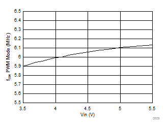
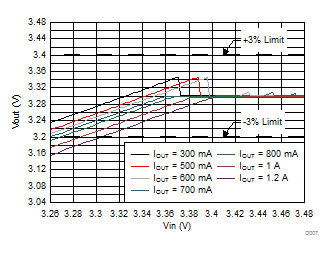
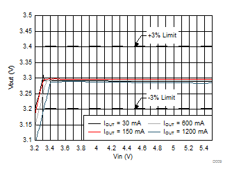
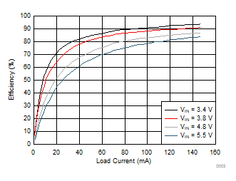
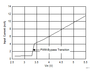
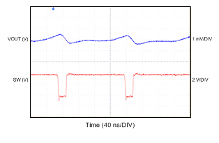
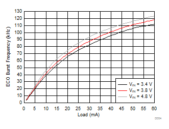
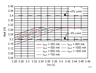
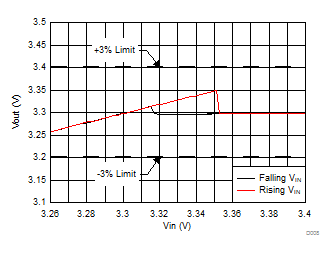
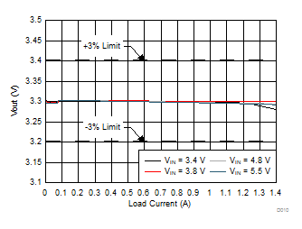
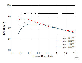
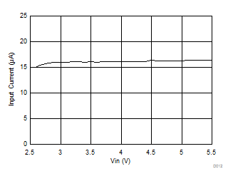
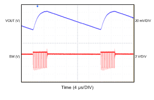
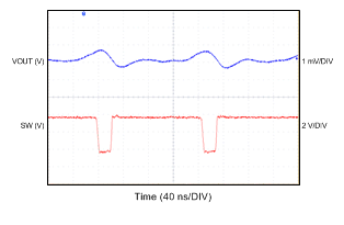
6.7 Typical Characteristics
All curves are at TA = 25°C and VIN = 3.8 V, unless otherwise specified. CIN, COUT = 2.2 µF, CLOAD2 = 4.7 µF, CLOAD1 = 10 µF, LSW = 0.47 µH.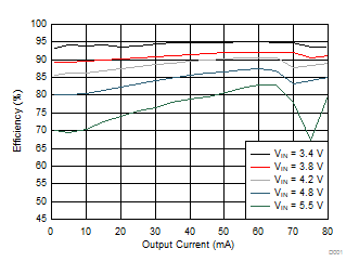
| IOUT = 100 mA |
| IOUT = 30 mA |
| IOUT = 10 mA |
| IOUT = 10 mA |