SNVSA38 November 2014 LM3281
PRODUCTION DATA.
- 1 Features
- 2 Applications
- 3 Description
- 4 Revision History
- 5 Pin Configuration and Functions
- 6 Specifications
- 7 Detailed Description
- 8 Application and Implementation
- 9 Power Supply Recommendations
- 10Layout
- 11Device and Documentation Support
- 12Mechanical, Packaging, and Orderable Information
5 Pin Configuration and Functions
DSBGA (YFQ)
6 Pins
Top
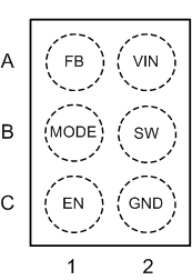
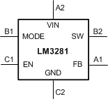 Figure 1. Pin Out
Pin Functions
| PIN | TYPE | DESCRIPTION | |
|---|---|---|---|
| NO. | NAME | ||
| A1 | FB | Power | Connect to the output at the output filter capacitor COUT by lowest inductance path with a trace rated for 2 A. |
| A2 | VIN | Power | Connect to input filter capacitor CIN by lowest inductance path, then connect to supply voltage with a trace rated for 2 A. |
| B1 | MODE | Logic | Selects automatic ECO/PWM mode or forced PWM mode. When MODE is HIGH the LM3281 automatically transitions between PWM and ECO operation. When MODE is LOW the LM3281 operates in PWM mode only. Do not leave MODE pin floating. |
| B2 | SW | Power | Connect to inductor LSW with a trace rated for 2 A. |
| C1 | EN | Logic | Set this digital input logic high for normal operation. For shutdown, set to logic low. Do not leave EN pin floating. |
| C2 | GND | Ground | Connect to input filter capacitor CIN by lowest inductance path, then to system ground by a very low inductance path. |