SNVSA38 November 2014 LM3281
PRODUCTION DATA.
- 1 Features
- 2 Applications
- 3 Description
- 4 Revision History
- 5 Pin Configuration and Functions
- 6 Specifications
- 7 Detailed Description
- 8 Application and Implementation
- 9 Power Supply Recommendations
- 10Layout
- 11Device and Documentation Support
- 12Mechanical, Packaging, and Orderable Information
8 Application and Implementation
NOTE
Information in the following applications sections is not part of the TI component specification, and TI does not warrant its accuracy or completeness. TI’s customers are responsible for determining suitability of components for their purposes. Customers should validate and test their design implementation to confirm system functionality.
8.1 Application Information
The LM3281 is a high efficiency DC-DC converter optimized to power Wireless Connectivity Solutions in cell phones, portable communication devices or other battery-powered RF devices. The device is designed to operate from an input supply voltage between 3 V and 5.5 V with a maximum load current of 1.2 A. It operates in PWM mode for medium to heavy load conditions and in ECO mode for light load conditions to optimize for best efficiency , transient performance and output voltage ripple at varying load conditions. In PWM mode the LM3281 converter operates with nominal switching frequency of 6 MHz, thus enabling use of smaller size capacitors and inductor. The converter operates in ECO mode at lighter load conditions to maintain high efficiency. In this mode a period of switching burst charges the output capacitor to the regulation target. This is followed by a period of no switching where the output voltages coasts to a lower voltage threshold due to light load current consumption. Upon reaching this lower voltage threshold, the cycle repeats by starting a new switching burst. The LM3281 automatically transitions into Analog Bypass operation as input voltage approaches output voltage.
Figure 17 shows one of many application configurations for LM3281. A battery-connected system boost bypass (normally part of system PMU) provides input supply to LM3281 which in turn very efficiently converts this input to a fixed 3.3-V output with superior transient response and output noise, thereby saving the Wireless Connectivity Solution from having to operate from a higher supply voltage, such as a direct connection to a battery or a system boost/bypass. This results in significant power dissipation savings and consequently cooler operation for the connectivity solution without sacrificing its RF performance. In applications where low voltage battery operation is not a significant feature, system boost/bypass can be eliminated, and the LM3281 can be directly connected to a battery for high efficiency power conversion and excellent RF performance. These types of always-on applications are feasible because of very low IQ of LM3281.
8.2 Typical Application
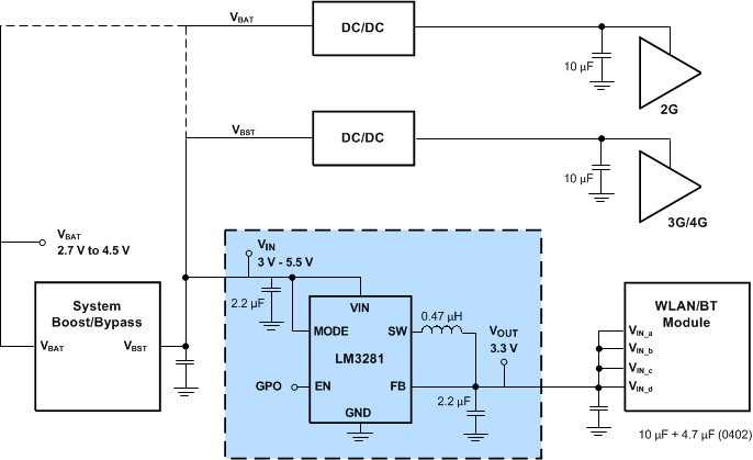 Figure 17. LM3281 Typical Application
8.2.1 Design Requirements
Design requirements for LM3281 pertain to the use of appropriate passive components. The recommended passive components (inductors and capacitors) are optimally selected to provide best performance for a typical application.
8.2.1.1 Suggested Passive Components
Referencing the Simplified Schematic on page 1, the LM3281 Inductor Selection, Total Effective Output Capacitance (COUT + CLOAD1 + CLOAD2), LM3281 Capacitor (CIN and COUT) Selection, Recommended Load Bypass Capacitors (CLOAD1 and CLOAD2), and Alternate Output Capacitor Configuration sections provide suggested passive components. Please consult the TI applications team to select suitable alternatives.
8.2.1.1.1 LM3281 Inductor Selection
The solution inductor shown in the Simplified Schematic can be optimized for size or solution efficiency. The 2012-size inductor listed below will perform well but other suitable smaller size inductors may be available in the future.
Table 3. Suggested Inductor
| INDUCTANCE | DCR | ISAT | SIZE | PART NUMBER | VENDOR | |
|---|---|---|---|---|---|---|
| LSW | 0.47 µH ± 20% | 40 mΩ | 2.4 A | 2.00 x 1.25 x 1.00 mm | LQM21PNR47MGH | Murata |
The inductor used in LM3281 designs should have following characteristics over operating temperature range:
- DC resistance (DCR) ≤ 70 mΩ
- Inductance at 0-mA current = 0.47 µH ±20%
- Inductance at 1.4-A current ≥ 0.29 µH
- Inductance at 2-A current ≥ 0.26 µH
If an application requires less than 1.4A peak load current, it is possible to trade maximum load current for DCR of the inductor (hence smaller physical size) by using Equation 1:
where DCR_IND_MAX is the maximum DC resistance of inductor in Ohms and I_MAX is the maximum load current in Amperes.
8.2.1.1.2 Total Effective Output Capacitance (COUT + CLOAD1 + CLOAD2)
Total effective output capacitance including load capacitance (CLOAD1 and CLOAD2) and solution capacitance (COUT), de-rated for 3.3-V DC bias, operating temperature range, aging, etc. must be 3.4 μF to 9 μF.
Table 4. Total Effective Output Capacitance
| MIN | TYP | MAX | UNIT | |
|---|---|---|---|---|
| Effective COUT (capacitor placed closest to LM3281), de-rated for 3.3-V DC bias, operating temperature and aging | 0.8 | 9 | μF | |
| Total effective output capacitance (COUT + CLOAD1 + CLOAD2), de-rated for 3.3-V DC bias, operating temperature range, and aging | 3.4 | 7 | 9 | μF |
8.2.1.1.3 LM3281 Capacitor (CIN and COUT) Selection
The LM3281 is designed for use with ceramic capacitors for its input and output filters. Ceramic capacitors types such as X5R, X7R are recommended for both filters. Note that suggested LM3281 solution capacitors are de-rated by 50% to 65% at 3.3-V DC bias.
Table 5. Suggested Capacitors
| CAPACITANCE | CAPACITANCE @3.3V DC BIAS |
SIZE (IMPERIAL) |
PART NUMBER | VENDOR | |
|---|---|---|---|---|---|
| CIN | 2.2 μF ± 10% | 1.1 µF | 0402, 0.50 mm height | CL05A225KQ5NNNC | Samsung |
| COUT | |||||
| CIN | 2.2 μF ± 20% | 0.8 µF | 0201, 0.30 mm height | CL03A225MQ3CRNC | Samsung |
| COUT |
8.2.1.1.4 Recommended Load Bypass Capacitors (CLOAD1 and CLOAD2)
Suggested load capacitors are de-rated by 55% to 60% at 3.3-V DC bias. Contact TI for additional recommendations regarding load bypass capacitor value and case sizes.
Table 6. Recommended Load Capacitors
| CAPACITANCE | CAPACITANCE @3.3V DC BIAS |
SIZE (IMPERIAL) |
PART NUMBER | VENDOR | |
|---|---|---|---|---|---|
| CLOAD1 | 10 μF ± 20% | 4.2 μF | 0402, 0.50 mm height | CL05A106MP5NUNC | Samsung |
| CLOAD1 | 10 μF ± 10% | 5.2 μF | 0603, 0.80 mm height | CL10A106KP8NNNC | Samsung |
| CLOAD2 | 4.7 μF ± 20% | 2 μF | 0402, 0.50 mm height | CL05A475MP5NRNC | Samsung |
8.2.1.1.5 Alternate Output Capacitor Configuration
If only one output capacitor is desired for minimum system solution size components in Table 7 can be used. In this case components COUT, CLOAD1, and CLOAD2 are absorbed into COUT; CLOAD1 and and CLOAD2 are eliminated. COUT must be placed very close to the LM3281.
Table 7. Other Recommended Capacitors
| CAPACITANCE | CAPACITANCE @3.3V DC BIAS |
SIZE (IMPERIAL) |
PART NUMBER | VENDOR | |
|---|---|---|---|---|---|
| COUT | 22 μF ± 20% | 7.3 μF | 0603, 0.80 mm height | GRM188R60J226MEA0D | Murata |
8.2.2 Detailed Design Procedure
The LM3281 is designed to use ceramic capacitors for its input and output filters. Use a 2.2-µF capacitor for input that provides a minimum of 0.8 µF effective capacitance under bias and worst-case temperature conditions. For output filter, combination of COUT, CLOAD1 and CLOAD2 should yield at least 3.4 µF (but not more than 9 µF) of effective capacitance under bias and worst-case temperature conditions. Please refer to Table 5, Table 6, and Table 7 for specific recommended components.
The input filter capacitor supplies AC current drawn by the PFET switch of the LM3281 in the first part of each cycle and reduces the voltage ripple imposed on the input power source. The output filter capacitor absorbs the AC inductor current, helps maintain a steady output voltage during transient load changes and reduces output voltage ripple. These capacitors must be selected with sufficiently low ESR (Equivalent Series Resistance) to perform these functions. The ESR of the filter capacitors is generally a major factor in voltage ripple.
There are two main considerations when choosing an inductor: the inductor should not saturate (inductance should not drop significantly with current), and DC resistance of the inductor should not be excessively high. Different manufacturers follow different saturation current rating specifications, so attention must be given to details. Saturation current ratings are typically specified at 25°C so ratings over the ambient temperature range of the application should be requested from the manufacturer. Refer to LM3281 Inductor Selection for a recommendation about a specific part number and other useful guidelines about inductor selection.
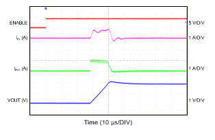
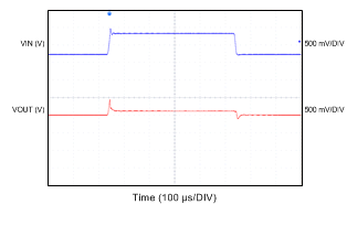
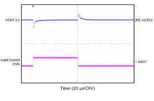
8.2.3 Application Curves
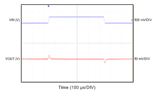
| 3.8 V → 4.2V → 3.8 V | IOUT = 600 mA | |
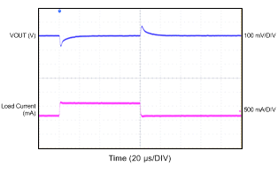
| PWM-PWM 150 mA → 600 mA → 150 mA | ||

| ECO-PWM-ECO 30 mA → 600 mA → 30 mA | ||
| IOUT = 1 mA | ||
| 3.2 V → 3.8 V → 3.2 V | IOUT = 600 mA | |
| PWM-PWM Heavy Step 150 mA →1200 mA → 150 mA | ||
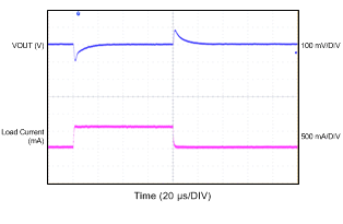
| Forced PWM 30 mA → 600 mA → 30 mA | ||
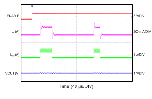
| Output shorted to Ground | ||