SNVSA38 November 2014 LM3281
PRODUCTION DATA.
- 1 Features
- 2 Applications
- 3 Description
- 4 Revision History
- 5 Pin Configuration and Functions
- 6 Specifications
- 7 Detailed Description
- 8 Application and Implementation
- 9 Power Supply Recommendations
- 10Layout
- 11Device and Documentation Support
- 12Mechanical, Packaging, and Orderable Information
7 Detailed Description
7.1 Overview
The LM3281 is a size- and performance-optimized step-down DC-DC converter for powering power amplifiers, front-end modules, wireless connectivity solutions, and a wide variety of other applications. The device complements the portfolio of SuPA (Supply for PA) products by combining small solution size, low dropout analog bypass with smooth mode transitions, very low standby current for always-on applications, very low ripple with “forced PWM” mode operation, high maximum output current, ability to drive large load capacitance while retaining transient performance, and soft start to limit start-up current.
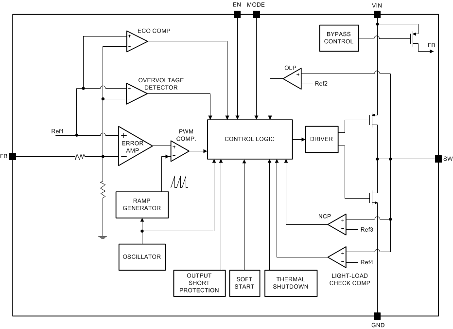
7.2 Functional Block Diagram
7.3 Feature Description
7.3.1 Small Solution Size
Solution size less than 7.5 mm2 is possible using the LM3281 in combination with only three small passive components.
7.3.2 Automatic Analog Bypass with Low Dropout
An internal bypass transistor under analog control automatically engages as VIN falls below the VOUT target. Output stays regulated in analog bypass mode until full dropout. The parallel impedance of this additional bypass transistor with normal DC-DC output path reduces VOUT voltage drop-out, maximizing VOUT supply voltage to the load at low VIN conditions. The analog implementation provides a smooth transition among regulation and bypass modes, avoiding VOUT distortion.
7.3.3 Low IQ
An ECOnomy (ECO) mode of operation draws 16 µA (typ.) quiescent current, permitting the LM3281 to be used in “always-on” applications. This low IQ is achieved over the entire input supply range of 5.5 V to 2.6 V, irrespective of whether LM3281 is operating in regulation (ECO Mode or Analog Bypass mode) or in full dropout (full bypass).
7.3.4 Forced PWM Operation
ECO mode provides low IQ while PWM mode optimizes output voltage ripple and transient performance. When high, the MODE pin permits automatic mode selection based on load current. When MODE is pulled low the LM3281 enters “forced PWM” operation with very low ripple and optimized transient response. Alternately, the MODE pin can be tied high in an application to allow the device to always select a mode of operation automatically.
7.3.5 High Maximum Current
Load current of 1.2 A is supported with short bursts (of < 100 µS with < 10% duty cycle) up to 1.4 A.
A wide variety of load current use cases are accommodated by the LM3281. Examples are described in Table 1 and Table 2: one for high ambient temperature all the time, and one for a more typical ambient temperature use case. Many alternate use case scenarios are available; please contact TI to discuss the load current relevant for a given application.
For the high ambient temperature of 85°C for the entire device operational lifetime, see Table 1:
Table 1. ILOAD Example for Constant 85°C Ambient Temperature
| ILOAD | AMBIENT TEMPERATURE | PERCENT OPERATIONAL LIFETIME |
|---|---|---|
| 100 mA | 85°C | Up to 100% |
| 700 mA | 85°C | Up to 60% |
| 1400 mA | 85°C | Up to 3% |
For a more typical ambient temperature distribution of TA ≤ 70°C for ≥ 80% of the operational lifetime and 70°C < TA ≤ 85% for ≤ 20% of the operational lifetime, see Table 2:
Table 2. ILOAD Example for a More Typical Ambient Temperature Use
| ILOAD | AMBIENT TEMPERATURE | PERCENT OPERATIONAL LIFETIME |
|---|---|---|
| 100 mA | 70°C < TA ≤ 85°C for ≤ 20% of time TA ≤ 70°C for ≥ 80% of time |
Up to 100% |
| 850 mA | 70°C < TA ≤ 85°C for ≤ 20% of time TA ≤ 70°C for ≥ 80% of time |
Up to 60% |
| 1400 mA | 70°C < TA ≤ 85°C for ≤ 20% of time TA ≤ 70°C for ≥ 80% of time |
Up to 3% |
7.3.6 High-Capacitance Load and Line Transient Performance
The LM3281 is internally compensated to drive loads with large bypass capacitance, including transceiver modules, without sacrificing transient performance. Please reference Total Effective Output Capacitance (COUT + CLOAD1 + CLOAD2) regarding output capacitance requirements.
7.3.7 Soft Start
During start-up a soft-start feature prevents high input current which could cause supply voltage bus drops and interfere with other subsystems sharing the supply bus. Soft start is especially valuable in applications where large load capacitance must be charged on start-up. Loading of the output during start-up condition will extend the soft-start time. Excessive loading may even prevent the output from reaching the target voltage, and the device may therefore stay in the soft-start condition indefinitely.
7.3.8 Thermal Overload Protection
The LM3281 device has a thermal overload protection that protects the device from short-term misuse and overload conditions. If the junction temperature exceeds 150°C, the LM3281 shuts itself down. Normal operation resumes after the temperature drops below 125°C. Prolonged operation in thermal overload condition may damage the device and is therefore not recommended.
7.3.9 Current Limit
The current limit feature allows the LM3281 to protect itself and external components during overload conditions. In PWM mode, the cycle-by-cycle current limit of the SW pin is 1.9-A peak, and the bypass current limit is 1.3 A. Thus, the total current limit is 2.2 A (typ.). During the start-up condition or when the output voltage is less than 0.34 V, the SW pin current limit is reduced to 0.85 A peak, and the bypass current is disabled. If excessive load prevents the output from rising above 0.34 V for more than 40 μs, the LM3281 enters the short-circuit-protection state.
7.3.10 Power-On Reset
Some applications may require tying the EN pin directly to the VIN pin. For this reason, the LM3281 features a Power on Reset (POR) that ensures that the part will enter a deterministic state when power is first applied. When the EN pin is tied directly to the VIN pin, the input power supply needs to rise fast enough for the POR circuit to work properly. The VIN voltage should not stay between 1.2 V and 2.6 V for longer than 20 µs. This is not required if the EN pin voltage remains below VIL (below 0.2 V) until VIN is at least at 2.6 V.
7.4 Device Functional Modes
The LM3281 includes five steady-state modes of operation depending on MODE, VIN, and ILOAD conditions: PWM (Pulse Width Modulation), Forced PWM, ECO (ECOnomy), Analog Bypass, and Shutdown. Two protection mechanisms include current limiting and thermal overload protection. Finally, soft-start operation is active to prevent excessive input current only when the part is first enabled.
7.4.1 PWM Mode
When the LM3281 operates in PWM mode, the switching frequency is constant, and the switcher regulates the output voltage by changing the energy per cycle to support the load required. During the first portion of each switching cycle, the control block in the LM3281 turns on the internal PFET switch. This allows current to flow from the input through the inductor and to the output filter capacitor and load. The inductor limits the current to a ramp with a slope of (VIN – VOUT)/L, by storing energy in its magnetic field. During the second portion of each cycle, the control block turns the PFET switch off, blocking current flow from the input, and then turns the NFET synchronous rectifier on. The inductor draws current from ground through the NFET and to the output filter capacitor and load, which ramps the inductor current down with a slope of –VOUT/L. The output filter capacitor stores charge when the inductor current is greater than the load current and releases it when the inductor current is less than the load current, smoothing the voltage across the load. At the next rising edge of the clock, the cycle repeats. An increase of load pulls the output voltage down, increasing the error signal. As the error signal increases, the peak inductor current becomes higher, thus increasing the average inductor current. The output voltage is therefore regulated by modulating the PFET switch on-time to control the average current sent to the load. The circuit generates a duty-cycle modulated rectangular signal that is averaged using a low pass filter formed by the inductor and output capacitor. The output voltage is equal to the average of the duty-cycle modulated rectangular signal.
7.4.2 Forced PWM (FPWM) Mode
To maintain high efficiency at lighter loads, LM3281 automatically goes into what is called ECO mode which has low IQ but higher ripple compared to PWM mode. If an application requires very low ripple and/or fast transient response, LM3281 can be forced to operate in PWM mode even at lighter loads. When high, the MODE pin permits automatic PWM or ECO mode operation based on load current. When MODE is pulled low the LM3281 enters “forced PWM” operation with very low ripple and optimized transient response. If automatic PWM/ECO mode operation is desired, the MODE pin can be permanently tied high in an application to allow the device to always select a mode of operation automatically based on the load current conditions.
It should be noted that LM3281 transient performance is quite good in ECO mode, and it may not be necessary to operate in FPWM mode for transient performance reasons alone. Normally, FPWM operation is selected for lower output voltage ripple.
7.4.3 Analog Bypass Mode
The LM3281 contains an internal BPFET (Bypass FET) transistor connected from the battery directly to the output for bypassing the PWM DC-DC converter when VIN approaches VOUT. In Analog Bypass mode, this BPFET is turned on just enough for the PWM DC-DC to maintain regulation by providing a parallel path from the battery directly to the load for maximum usable battery range and extended operating time while maintaining regulation. When the part is in dropout and is operating in full bypass mode, the output voltage will be the input voltage less the voltage drop across the resistance of the BPFET in parallel with the PFET + Switch Inductor. Analog Bypass mode is more efficient than operating in PWM mode at 100% duty cycle because the combined resistance of the circuit is significantly less than the series resistance of just the PWM PFET and inductor. This translates into higher voltage available at the output in Analog Bypass mode for a given battery voltage. The bypass operation is very system resource friendly in that the bypass PFET is gradually turned on automatically when the input voltage gets close to the output voltage (while always maintaining regulation), a typical scenario of a discharging battery. Likewise, it is also automatically gradually turned off when the input voltage rises, a typical scenario when connecting a charger.
7.4.4 ECO (Economy) Mode
At light load current, the converter enters ECO mode operation with reduced quiescent supply current to maintain high efficiency. During ECO mode operation, a switching burst brings the output just above target voltage. This period of switching is followed by no switching in which the output coasts to just below target voltage, and then this cycle is repeated. The frequency of how often the switching burst occurs is dependent on the load current. PWM operation resumes once the load current reaches a specific threshold.
7.4.5 Shutdown Mode
Setting the EN digital input pin low (< 0.4 V) places the LM3281 in Shutdown mode where it consumes less than 0.1 μA current typically. In shutdown, the PFET switch, the NFET synchronous rectifier, the BPFET, reference voltage source, control, and bias circuitry of the LM3281 are turned off. Setting EN high (> 1.2 V) enables normal operation.