SNVSA38 November 2014 LM3281
PRODUCTION DATA.
- 1 Features
- 2 Applications
- 3 Description
- 4 Revision History
- 5 Pin Configuration and Functions
- 6 Specifications
- 7 Detailed Description
- 8 Application and Implementation
- 9 Power Supply Recommendations
- 10Layout
- 11Device and Documentation Support
- 12Mechanical, Packaging, and Orderable Information
10 Layout
10.1 Layout Guidelines
Optimal LM3281 performance is realized when two important layout considerations are observed. TI-provided layout guidance in this section illustrates best practices, and a customer layout review with the TI applications team will ensure best performance is achieved.
10.1.1 COUT-to-CLOAD Inductance
Minimize inductance in the path between LM3281 COUT capacitor and the load bypass capacitors CLOAD1 and CLOAD2 for best performance. Total power path inductance from the LM3281 output to the load (including vias and traces) should target < 1 nH and must not exceed 2 nH.
10.1.2 LM3281-to-CIN Inductance
Minimize inductance between LM3281 pins (VIN, GND) and the LM3281 input bypass capacitor CIN for best performance. The LM3281 device and CIN capacitor should be placed to permit shortest possible top-metal routing for these connections.
Poor board layout can disrupt the performance of a DC-DC converter and surrounding circuitry by contributing to EMI, ground bounce, and resistive voltage loss in the traces resulting in poor regulation or instability. Poor layout can also result in re-flow problems leading to poor solder joints between the DSBGA package and board pads which can result in erratic or degraded performance of the converter. By its very nature, any switching converter generates electrical noise, and the circuit board designer’s challenge is to minimize, contain, or attenuate such switcher-generated noise. A high-frequency switching converter, such as the LM3281, switches Ampere level currents within nanoseconds, and the traces interconnecting the associated components can act as radiating antennas. The following general guidelines are offered to help mitigate EMI and facilitate good layout design.
- Place the LM3281 switcher, its input capacitor, and output filter inductor and capacitor close together, and make the Inter-connecting traces as short as possible.
- Arrange the components so that the switching current loops curl in the same direction. During the first half of each cycle, current flows from the input filter capacitor, through the internal PFET of the LM3281 and the inductor, to the output filter capacitor, then back through ground, forming a current loop. In the second half of each cycle, current is pulled up from ground, through the internal synchronous NFET of the LM3281 by the inductor, to the output filter capacitor and then back through ground, forming a second current loop. Routing these loops so the current curls in the same direction prevents magnetic field reversal between the two half-cycles and reduces radiated noise.
- Make the current loop area(s) as small as possible.
- Reduce the amount of switching current that circulates through the ground plane: Connect the ground bump of the LM3281 and its input filter capacitor together using generous component-side copper fill as a pseudo-ground plane. Then connect this copper fill to the system ground-plane (if one is used) with multiple vias. These multiple vias help to minimize ground bounce at the LM3281 by giving it a low-impedance ground connection.
- Minimize resistive losses by using wide traces between the power components and doubling up traces on multiple layers when needed.
- Route noise sensitive traces, such as the voltage feedback path, as directly as possible from the switcher FB pad to the VOUT pad of the output capacitor, but keep it away from noisy traces between the power components.
- Take advantage of the inherent inductance of circuit traces to reduce coupling among various function blocks on the board, by way of the power supply traces.
10.2 Layout Example
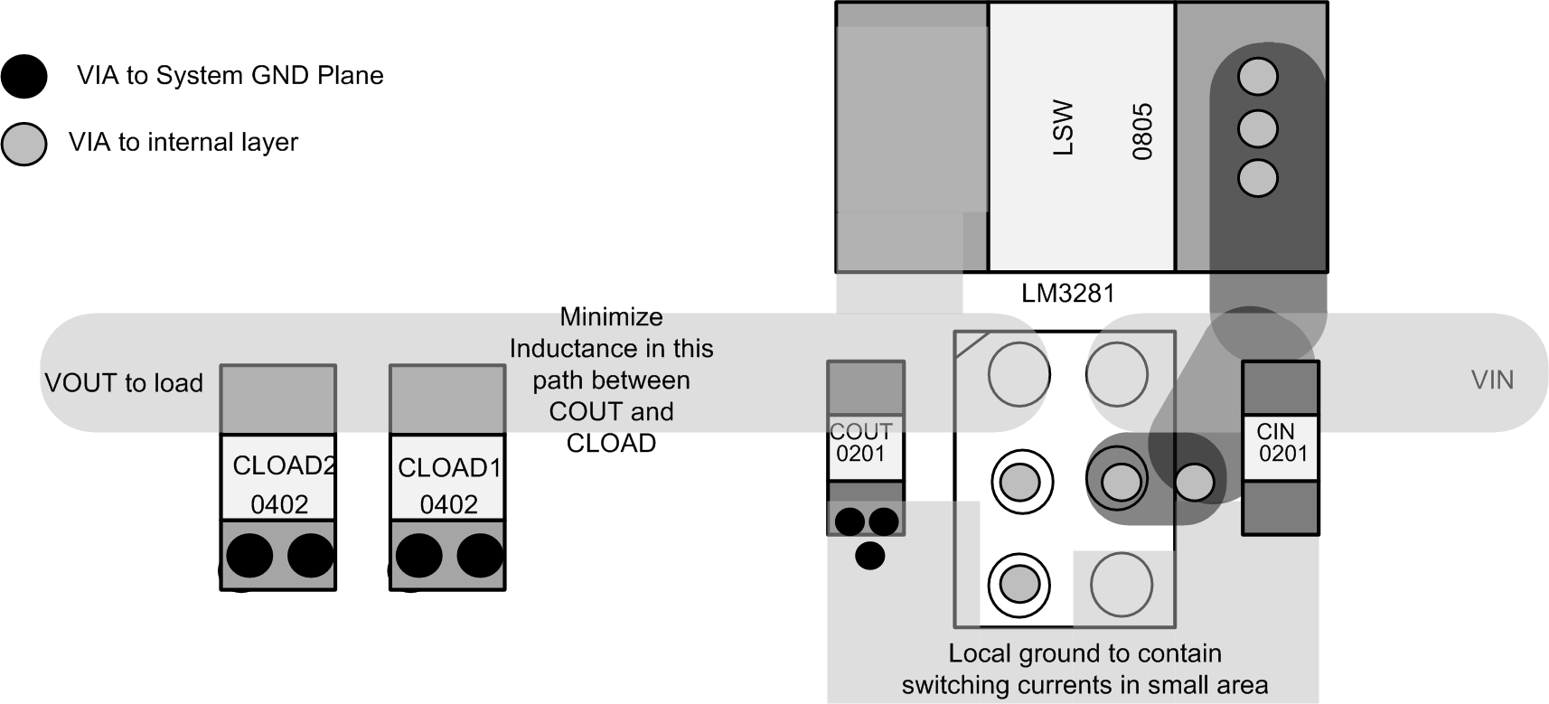 Figure 26. LM3281 Layout Example
10.3 DSBGA Package Assembly And Use
Use of the DSBGA package requires specialized board layout, precision mounting, and careful re-flow techniques, as detailed in Texas Instruments Application Note 1112 DSBGA Wafer Level Chip Scale Package (SNVA009). Refer to the section Surface Mount Technology (SMD) Assembly Considerations. For best results in assembly, alignment ordinals on the PC board should be used to facilitate placement of the device. The pad style used with DSBGA package should be the NSMD (non-solder mask defined) type. This means that the solder-mask opening is larger than the pad size. This prevents a lip that otherwise forms if the solder-mask and pad overlap from holding the device off the surface of the board and interfering with mounting. See Application Note 1112 for specific instructions how to do this.
The DSBGA package is optimized for the smallest possible size in applications with red or infrared opaque cases. Because the DSBGA package lacks the plastic encapsulation characteristic of larger devices, it is vulnerable to light. Backside metallization and/or epoxy coating, along with front-side shading by the printed circuit board, reduce this sensitivity. However, the package has exposed die edges. In particular, DSBGA devices are sensitive to light (in the red and infrared range) shining on the package's exposed die edges.