ZHCSH33Z September 1997 – April 2025 LM317
PRODUCTION DATA
- 1
- 1 特性
- 2 应用
- 3 说明
- 4 Device Comparison Table
- 5 Pin Configuration and Functions
- 6 Specifications
- 7 Detailed Description
-
8 Application and Implementation
- 8.1 Application Information
- 8.2 Typical Application
- 8.3
System Examples
- 8.3.1 0V to 30V Regulator Circuit
- 8.3.2 Adjustable Regulator Circuit With Improved Ripple Rejection
- 8.3.3 Precision Current-Limiter Circuit
- 8.3.4 Tracking Preregulator Circuit
- 8.3.5 1.25V to 20V Regulator Circuit With Minimum Program Current
- 8.3.6 Battery-Charger Circuit
- 8.3.7 50mA, Constant-Current, Battery-Charger Circuit
- 8.3.8 Slow Turn-On 15V Regulator Circuit
- 8.3.9 AC Voltage-Regulator Circuit
- 8.3.10 Current-Limited 6V Charger Circuit
- 8.3.11 Adjustable 4A Regulator Circuit
- 8.3.12 High-Current Adjustable Regulator Circuit
- 8.4 Power Supply Recommendations
- 8.5 Layout
- 9 Device and Documentation Support
- 10Revision History
- 11Mechanical, Packaging, and Orderable Information
封装选项
机械数据 (封装 | 引脚)
散热焊盘机械数据 (封装 | 引脚)
订购信息
8.5.1.1.2.1 Heatsinking the SOT-223 (DCY) Package
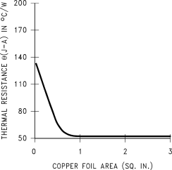
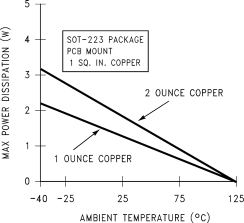
Figure 8-19 and Figure 8-20 show information for the SOT-223 package. Figure 8-20 assumes a RθJA of 74°C/W for 1oz. copper and 59.6°C/W for 2oz. copper (further details are in Section 6.5) and a maximum junction temperature of 125°C. See the AN-1028 Maximum Power Enhancement Techniques for Power Packages application note for thermal enhancement techniques to be used with the SOT-223 and TO-252 packages.
 Figure 8-19 RθJA vs Copper (2oz.) Area for the
SOT-223 Package
 Figure 8-20 Maximum Power Dissipation vs TAMB for the SOT-223 Package