ZHCS529I January 2007 – April 2025 LM25574
PRODUCTION DATA
- 1
- 1 特性
- 2 应用
- 3 说明
- 4 Pin Configuration and Functions
- 5 Specifications
- 6 Detailed Description
-
7 Application and Implementation
- 7.1 Application Information
- 7.2
Typical Application
- 7.2.1 Typical Schematic for High Frequency (1MHz) Application
- 7.2.2 Design Requirements
- 7.2.3
Detailed Design Procedure
- 7.2.3.1 Custom Design With WEBENCH® Tools
- 7.2.3.2 External Components
- 7.2.3.3 R3 -RT Resistor
- 7.2.3.4 L1-Inductor
- 7.2.3.5 C3 (CRAMP)
- 7.2.3.6 C9-Output Capacitor
- 7.2.3.7 C1-Input Capacitor
- 7.2.3.8 C8- VCC Capacitor
- 7.2.3.9 C7- BST capacitor
- 7.2.3.10 C4 - SS Capacitor
- 7.2.3.11 R5, R6 - Feedback Resistor
- 7.2.3.12 R1, R2, C2 - SD Pin Components
- 7.2.3.13 R4, C5, C6 - Compensation Components
- 7.2.3.14 Bias Power Dissipation Reduction
- 7.2.4 Application Curves
- 7.3 Power Supply Recommendations
- 7.4 Layout
- 8 Device and Documentation Support
- 9 Revision History
- 10Mechanical, Packaging, and Orderable Information
7.2.3.4 L1-Inductor
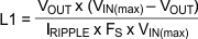
The inductor value is determined based on the operating frequency, load current, ripple current, and the minimum and maximum input voltage (VIN(min), VIN(max)).
 Figure 7-2 Inductor Current Waveform
To keep the circuit in continuous conduction mode (CCM), the maximum ripple current IRIPPLE must be less than twice the minimum load current, or 0.2 Ap-p. Using this value of ripple current, the value of inductor (L1) is calculated using the following:
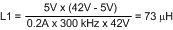
This procedure provides a guide to select the value of L1. The nearest standard value (100µH) is used. L1 must be rated for the peak current (IPK+) to prevent saturation. During normal loading conditions, the peak current occurs at maximum load current plus maximum ripple. During an overload condition the peak current is limited to 0.7A nominal (0.85A maximum). The selected inductor (see Equation 7) has a conservative 1.0 Amp saturation current rating. For this manufacturer, the saturation rating is defined as the current necessary for the inductance to reduce by 30%, at 20°C.