ZHCSNL9A May 2021 – December 2021 ISOW1044
PRODUCTION DATA
- 1 特性
- 2 应用
- 3 说明
- 4 Revision History
- 5 说明(续)
- 6 Device Comparison Table
- 7 Pin Configuration and Functions
-
8 Specifications
- 8.1 Absolute Maximum Ratings
- 8.2 ESD Ratings
- 8.3 Recommended Operating Conditions
- 8.4 ThermalInformation
- 8.5 Power Ratings
- 8.6 Insulation Specifications
- 8.7 Safety-Related Certifications
- 8.8 Safety Limiting Values
- 8.9 Electrical Characteristics
- 8.10 Supply Current Characteristics
- 8.11 Switching Characteristics
- 8.12 Insulation Characteristics Curves
- 8.13 Typical Characteristics
- 9 Parameter Measurement Information
- 10Detailed Description
- 11Application and Implementation
- 12Power Supply Recommendations
- 13Layout
- 14Device and Documentation Support
- 15Mechanical, Packaging, and Orderable Information
7 Pin Configuration and Functions
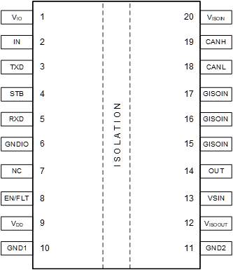
 Figure 7-1 ISOW104420-pin DFMTop View
Table 7-1 Pin Functions
| PIN | I/O | DESCRIPTION | |
|---|---|---|---|
| NAME | NO. | ||
| VIO | 1 | -- | Side 1 Logic supply |
| IN | 2 | I | General purpose logic (GPIO) input (internal pull-down) |
| TXD | 3 | I | Driver enable. If this pin is floating, the driver is disabled (internal pull-down) |
| STB | 4 | I | Standby enable. Connect this pin to GNDIO in normal mode. If this pin is floating or logic high, driver is in standby mode. |
| RXD | 5 | O | Receiver data output |
| GNDIO | 6 | -- | Ground connection on side 1 for VIO. GNDIO and GND1 are not internally connected and need be shorted on PCB. |
| NC | 7 | -- | Not connected internally |
| EN/FLT | 8 | I/O |
Multi-function power converter enable input pin or fault output pin. Can only be used as either an input pin or an output pin.
|
| VDD | 9 | -- | Side 1 DC-DC converter power supply |
| GND1 | 10 | -- | Ground connections on side for VDD . GNDIO and GND1 are not internally connected and need be shorted on PCB. |
| GND2 | 11 | -- | Ground connections on side for VISOOUT . GND2 and GISOIN are not internally connected and need be shorted direclty on PCB, or connected through a ferrite bead. |
| VISOOUT | 12 | -- | Isolated power converter output voltage. VISOOUT and VISOIN need be shorted directly on PCB, or connected through a ferrite bead. |
| VSIN | 13 | I | Power converter input . Pin 12 and pin 13 need be shorted directly on PCB. |
| OUT | 14 | O | General purpose logic (GPIO) output (default output is low) |
| GISOIN | 15, 16, 17 | -- | Ground connections for VISOIN. GND2 and GISOIN need be shorted direclty on PCB, or connected through a ferrite bead. |
| CANL | 18 | I/O | Low-level CAN bus line |
| CANH | 19 | I/O | High-level CAN bus line |
| VISOIN | 20 | -- | Power supply input for CAN tranceiver. VISOIN and VISOOUT need be shorted direclty on PCB, or connected through a ferrite bead. |