ZHCSFB4A July 2016 – January 2024 DS90UB964-Q1
PRODUCTION DATA
- 1
- 1特性
- 2应用
- 3说明
- Pin Configuration and Functions
-
4Specifications
- 4.1 Absolute Maximum Ratings
- 4.2 ESD Ratings – JEDEC
- 4.3 ESD Ratings – IEC and ISO
- 4.4 Recommended Operating Conditions
- 4.5 Thermal Information
- 4.6 DC Electrical Characteristics
- 4.7 AC Electrical Characteristics
- 4.8 Recommended Timing for the Serial Control Bus
- 4.9 AC Electrical Characteristics
- 4.10 Typical Characteristics
-
5Detailed Description
- 5.1 Overview
- 5.2 Functional Block Diagram
- 5.3 Feature Description
- 5.4
Device Functional Modes
- 5.4.1 RAW Data Type Support and Rates
- 5.4.2 MODE Pin
- 5.4.3 REFCLK
- 5.4.4 Receiver Port Control
- 5.4.5 Input Jitter Tolerance
- 5.4.6 Adaptive Equalizer
- 5.4.7 Channel Monitor Loop-Through Output Driver
- 5.4.8 RX Port Status
- 5.4.9 GPIO Support
- 5.4.10 RAW Mode LV / FV Controls
- 5.4.11 Video Stream Forwarding
- 5.4.12 CSI-2 Protocol Layer
- 5.4.13 CSI-2 Short Packet
- 5.4.14 CSI-2 Long Packet
- 5.4.15 CSI-2 Data Identifier
- 5.4.16 Virtual Channel and Context
- 5.4.17 CSI-2 Mode Virtual Channel Mapping
- 5.4.18 CSI-2 Transmitter Frequency
- 5.4.19 CSI-2 Transmitter Status
- 5.4.20 Video Buffers
- 5.4.21 CSI-2 Line Count and Line Length
- 5.4.22 FrameSync Operation
- 5.4.23
CSI-2 Forwarding
- 5.4.23.1 Best-Effort Round Robin CSI-2 Forwarding
- 5.4.23.2 Synchronized CSI-2 Forwarding
- 5.4.23.3 Basic Synchronized CSI-2 Forwarding
- 5.4.23.4 Line-Interleaved CSI-2 Forwarding
- 5.4.23.5 Line-Concatenated CSI-2 Forwarding
- 5.4.23.6 CSI-2 Replicate Mode
- 5.4.23.7 CSI-2 Transmitter Output Control
- 5.4.23.8 Enabling and Disabling CSI-2 Transmitters
- 5.5
Programming
- 5.5.1 Serial Control Bus
- 5.5.2 Second I2C Port
- 5.5.3 I2C Target Operation
- 5.5.4 Remote Target Operation
- 5.5.5 Remote Target Addressing
- 5.5.6 Broadcast Write to Remote Devices
- 5.5.7 I2C Proxy Controller
- 5.5.8 I2C Proxy Controller Timing
- 5.5.9 Interrupt Support
- 5.5.10 Timestamp – Video Skew Detection
- 5.5.11 Pattern Generation
- 5.5.12 FPD-Link BIST Mode
- 5.6 Register Maps
- 6Application and Implementation
- 7Device and Documentation Support
- 8Revision History
- 9Mechanical, Packaging, and Orderable Information
6.1.1 Power-Over-Coax
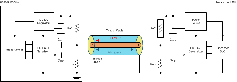
The DS90UB964-Q1 is designed to support the Power-over-Coax (PoC) method of powering remote sensor systems. With this method, the power is delivered over the same medium (a coaxial cable) used for high-speed digital video data and bidirectional control and diagnostics data transmission. The method uses passive networks or filters that isolate the transmission line from the loading of the DC-DC regulator circuits and their connecting power traces on both sides of the link as shown in Figure 6-1.
 Figure 6-1 Power-over-Coax (PoC) System Diagram
The PoC networks' impedance of ≥ 1kΩ over a specific frequency band is recommended to isolate the transmission line from the loading of the regulator circuits provided good layout practices are followed and the PCB return loss requirements given in Table 6-2 are met. Higher PoC network impedance contributes to favorable insertion loss and return loss characteristics in the high-speed channel. The lower limit of the frequency band is defined as ½ of the frequency of the back channel, fBC. The upper limit of the frequency band is the frequency of the forward high-speed channel, fFC. However, the main criteria that need to be met in the total high-speed channel, which consists of a serializer PCB, a deserializer PCB, and a cable, are the insertion loss and return loss limits defined in the Total Channel Requirements (see Section 5.4.6.1), while the system is under maximum current load and extreme temperature conditions.
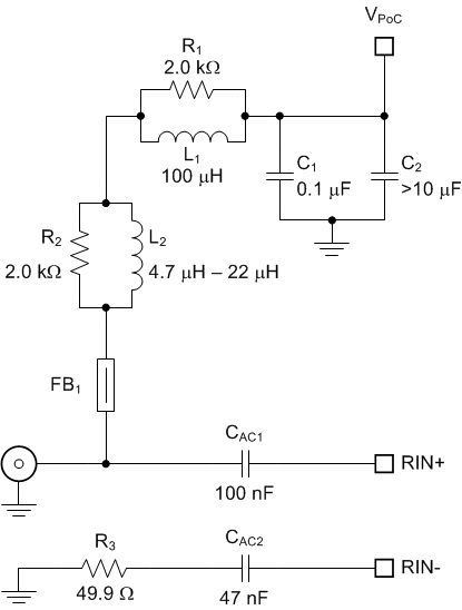
Figure 6-2 shows a PoC network recommended for a "2G" FPD-Link III consisting of a DS90UB913A-Q1 or DS90UB933-Q1 serializer and DS90UB964-Q1 with the bidirectional channel operating at the data rate of 2.5Mbps (½ fBC = 1.25MHz) and the forward channel operating at the data rate as high as 1.87Gbps (fFC ≈ 1GHz).
 Figure 6-2 Example Recommended PoC Network for a "2G"
FPD-Link III
Figure 6-2 Example Recommended PoC Network for a "2G"
FPD-Link IIITable 6-1 lists essential components for this particular PoC network.
| Count | Ref Des | Description | Part Number | MFR |
|---|---|---|---|---|
| 1 | L1 | Inductor, 100µH, 0.310Ω max, 710mA MIN (Isat, Itemp) 7.2MHz SRF typ, 6.6mm × 6.6mm, AEC-Q200 | MSS7341-104ML | Coilcraft |
| Inductor, 100µH, 0.606Ω max, 750mAMIN (Isat, Itemp) 7.2MHz SRF typ, 6.0mm × 6.0mm, AEC-Q200 | NRS6045T101MMGKV | Taiyo Yuden | ||
| 1 | L2 | Inductor, 4.7µH, 0.350Ω max, 700mA MIN (Isat, Itemp) 160MHz SRF typ, 3.8mm × 3.8mm, AEC-Q200 | 1008PS-472KL | Coilcraft |
| Inductor, 4.7µH, 0.130Ω max, 830mA MIN (Isat, Itemp), 70MHz SRF typ, 3.2mm × 2.5mm, General Purpose | CBC3225T4R7MRV | Taiyo Yuden | ||
| Inductor, 10µH, 0.288Ω max, 530mA MIN (Isat, Itemp) 30MHz SRF min, 3mm × 3mm, AEC-Q200 | LQH3NPZ100MJR | Murata | ||
| 1 | FB1 | Ferrite Bead, 1500kΩ at 1GHz, 0.5Ω max at DC 500mA at 85°C, SM0603, General Purpose | BLM18HE152SN1 | Murata |
| Ferrite Bead, 1500kΩ at 1GHz, 0.5Ω max at DC 500mA at 85°C, SM0603, AEC-Q200 | BLM18HE152SZ1 | Murata |
Application report Sending Power over Coax in DS90UB913A Designs (SNLA224) discusses and defines the PoC networks in more detail.
In addition to the PoC network components selection, the placement and layout play a critical role as well.
- Place the smallest component, typically a ferrite bead or a chip inductor, as close to the connector as possible. Route the high-speed trace through one of the ferrite bead pads to avoid stubs.
- Use the smallest component pads as allowed by manufacturer's design rules. Add anti-pads in the inner planes below the component pads to minimize impedance drop.
- Consult with connector manufacturer for optimized connector footprint.
- Use coupled 100Ω differential signal traces from the device pins to the AC-coupling caps. Use 50Ω single-ended traces from the AC-coupling capacitors to the connector.
- Terminate the inverting signal traces close to the connectors with standard 49.9Ω resistors.
The suggested characteristics for single-ended PCB traces (microstrips or striplines) for serializer or deserializer boards are detailed in Table 6-2. The effects of the PoC networks need to be accounted for when testing the traces for compliance to the suggested limits.
| PARAMETER | MIN | TYP | MAX | UNIT | ||
|---|---|---|---|---|---|---|
| Ltrace | Single-ended PCB trace length from the device pin to the connector pin | 5 | cm | |||
| Ztrace | Single-ended PCB trace characteristic impedance | 45 | 50 | 55 | Ω | |
| Zcon | Connector (mounted) characteristic impedance | 40 | 50 | 62.5 | Ω | |
| RL | Return Loss, S11 | ½ fBC < f < 0.1GHz | –20 | dB | ||
| 0.1GHz < f < 1GHz (f in GHz) | –12 + 8 × log(f) | dB | ||||
| 1GHz < f < fFC | –12 | dB | ||||
| IL | Insertion Loss, S12 | f < 0.5GHz | –0.35 | dB | ||
| f = 1GHz | –0.6 | dB | ||||
The VPOC noise must be kept to 10mVp-p or lower on the source / deserializer side of the system. The VPOC fluctuations on the serializer side, caused by the sensor's transient current draw and the DC resistance of cables and PoC components, must be kept at minimum as well. Increasing the VPOC voltage and adding extra decoupling capacitance (> 10µF) help reduce the amplitude and slew rate of the VPOC fluctuations.