ZHCSFB4A July 2016 – January 2024 DS90UB964-Q1
PRODUCTION DATA
- 1
- 1特性
- 2应用
- 3说明
- Pin Configuration and Functions
-
4Specifications
- 4.1 Absolute Maximum Ratings
- 4.2 ESD Ratings – JEDEC
- 4.3 ESD Ratings – IEC and ISO
- 4.4 Recommended Operating Conditions
- 4.5 Thermal Information
- 4.6 DC Electrical Characteristics
- 4.7 AC Electrical Characteristics
- 4.8 Recommended Timing for the Serial Control Bus
- 4.9 AC Electrical Characteristics
- 4.10 Typical Characteristics
-
5Detailed Description
- 5.1 Overview
- 5.2 Functional Block Diagram
- 5.3 Feature Description
- 5.4
Device Functional Modes
- 5.4.1 RAW Data Type Support and Rates
- 5.4.2 MODE Pin
- 5.4.3 REFCLK
- 5.4.4 Receiver Port Control
- 5.4.5 Input Jitter Tolerance
- 5.4.6 Adaptive Equalizer
- 5.4.7 Channel Monitor Loop-Through Output Driver
- 5.4.8 RX Port Status
- 5.4.9 GPIO Support
- 5.4.10 RAW Mode LV / FV Controls
- 5.4.11 Video Stream Forwarding
- 5.4.12 CSI-2 Protocol Layer
- 5.4.13 CSI-2 Short Packet
- 5.4.14 CSI-2 Long Packet
- 5.4.15 CSI-2 Data Identifier
- 5.4.16 Virtual Channel and Context
- 5.4.17 CSI-2 Mode Virtual Channel Mapping
- 5.4.18 CSI-2 Transmitter Frequency
- 5.4.19 CSI-2 Transmitter Status
- 5.4.20 Video Buffers
- 5.4.21 CSI-2 Line Count and Line Length
- 5.4.22 FrameSync Operation
- 5.4.23
CSI-2 Forwarding
- 5.4.23.1 Best-Effort Round Robin CSI-2 Forwarding
- 5.4.23.2 Synchronized CSI-2 Forwarding
- 5.4.23.3 Basic Synchronized CSI-2 Forwarding
- 5.4.23.4 Line-Interleaved CSI-2 Forwarding
- 5.4.23.5 Line-Concatenated CSI-2 Forwarding
- 5.4.23.6 CSI-2 Replicate Mode
- 5.4.23.7 CSI-2 Transmitter Output Control
- 5.4.23.8 Enabling and Disabling CSI-2 Transmitters
- 5.5
Programming
- 5.5.1 Serial Control Bus
- 5.5.2 Second I2C Port
- 5.5.3 I2C Target Operation
- 5.5.4 Remote Target Operation
- 5.5.5 Remote Target Addressing
- 5.5.6 Broadcast Write to Remote Devices
- 5.5.7 I2C Proxy Controller
- 5.5.8 I2C Proxy Controller Timing
- 5.5.9 Interrupt Support
- 5.5.10 Timestamp – Video Skew Detection
- 5.5.11 Pattern Generation
- 5.5.12 FPD-Link BIST Mode
- 5.6 Register Maps
- 6Application and Implementation
- 7Device and Documentation Support
- 8Revision History
- 9Mechanical, Packaging, and Orderable Information
5.4.5 Input Jitter Tolerance
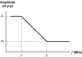
Input jitter tolerance is the ability of the clock and data recovery (CDR) and phase-locked loop (PLL) of the receiver to track and recover the incoming serial data stream. Jitter tolerance at a specific frequency is the maximum jitter permissible before data errors occur. Figure 5-3 shows the allowable total jitter of the receiver inputs and must be less than the values in Table 5-4.
 Figure 5-3 Input Jitter Tolerance Plot
Table 5-4 Input Jitter Tolerance Limit
| INTERFACE | JITTER AMPLITUDE (UI p-p) | FREQUENCY (MHz) (1) | ||
|---|---|---|---|---|
| FPD3 | A1 | A2 | ƒ1 | ƒ2 |
| 1 | 0.4 | FPD3_PCLK / 80 | FPD3_PCLK / 15 | |
(1) FPD3_PCLK frequency is a function of the PCLK, CLK_IN, or REFCLK frequency and
dependent on the serializer operating MODE: 10-bit mode: FPD3_PCLK = PCLK / 2
RAW 12-bit HF mode: FPD3_PCLK = 2 x PCLK / 3
RAW 12-bit LF mode: FPD3_PCLK = PCLK
RAW 12-bit HF mode: FPD3_PCLK = 2 x PCLK / 3
RAW 12-bit LF mode: FPD3_PCLK = PCLK