ZHCSKG3B September 2016 – February 2024 DS280DF810
PRODUCTION DATA
- 1
- 1 特性
- 2 应用
- 3 说明
- 4 Pin Configuration and Functions
-
5 Specifications
- 5.1 Absolute Maximum Ratings
- 5.2 ESD Ratings
- 5.3 Recommended Operating Conditions
- 5.4 Thermal Information
- 5.5 Electrical Characteristics
- 5.6 Timing Requirements, Retimer Jitter Specifications
- 5.7 Timing Requirements, Retimer Specifications
- 5.8 Timing Requirements, Recommended Calibration Clock Specifications
- 5.9 Recommended SMBus Switching Characteristics (Target Mode)
- 5.10 Recommended SMBus Switching Characteristics (Controller Mode)
- 5.11 Typical Characteristics
-
6 Detailed Description
- 6.1 Overview
- 6.2 Functional Block Diagram
- 6.3
Feature Description
- 6.3.1
Device Data Path Operation
- 6.3.1.1 AC-Coupled Receiver and Transmitter
- 6.3.1.2 Signal Detect
- 6.3.1.3 Continuous Time Linear Equalizer (CTLE)
- 6.3.1.4 Variable Gain Amplifier (VGA)
- 6.3.1.5 2x2 Cross-Point Switch
- 6.3.1.6 Decision Feedback Equalizer (DFE)
- 6.3.1.7 Clock and Data Recovery (CDR)
- 6.3.1.8 Calibration Clock
- 6.3.1.9 Differential Driver with FIR Filter
- 6.3.2 Debug Features
- 6.3.1
Device Data Path Operation
- 6.4 Device Functional Modes
- 6.5 Programming
- 6.6 Register Maps
- 7 Application and Implementation
- 8 Device and Documentation Support
- 9 Revision History
- 10Mechanical, Packaging, and Orderable Information
封装选项
请参考 PDF 数据表获取器件具体的封装图。
机械数据 (封装 | 引脚)
- ABW|135
- ABV|135
散热焊盘机械数据 (封装 | 引脚)
订购信息
6.3.1.9 Differential Driver with FIR Filter
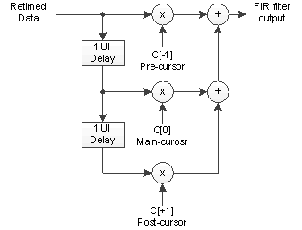
The DS280DF810 output driver has a three-tap finite impulse response (FIR) filter which allows for pre- and post-cursor equalization to compensate for a wide variety of output channel media. The filter consists of a weighted sum of three consecutive retimed bits as shown in the following diagram. C[0] can take on values in the range [-31, +31]. C[-1] and C[+1] can take on values in the range [-15, 15].
 Figure 6-3 FIR filter functional model
When utilizing the FIR filter, it is important to abide by the following general rules:
- |C[-1]| + |C[0]| + |C[+1]| ≤ 31; the FIR tap coefficients absolute sum must be less or equal to 31).
- sgn(C[-1]) = sgn(C[+1]) ≠ sgn(C[0]), for high-pass filter effect; the sign for the pre-cursor or post-cursor tap must be different from main-cursor tap to realize boost effect.
- sgn(C[-1]) = sgn(C[+1]) = sgn(C[0]), for low-pass filter effect; the sign for the pre-cursor or post-cursor tap must be equal to the main-cursor tap to realize attenuation effect.
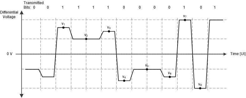
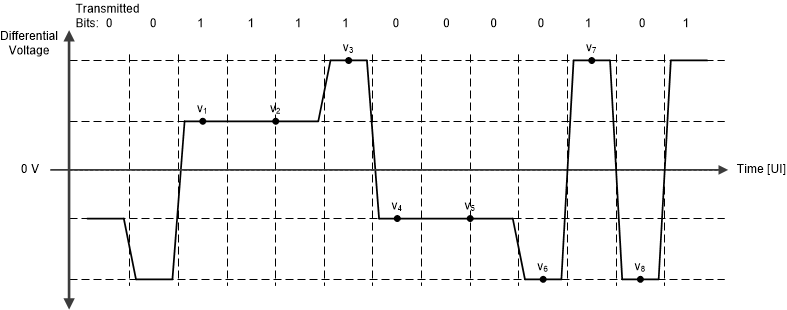
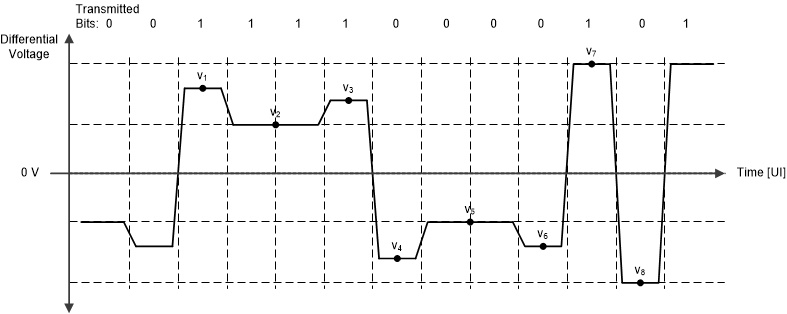
The FIR filter is used to pre-distort the transmitted waveform in order to compensate for frequency-dependant loss in the output channel. The most common way of pre-distorting the signal is to accentuate the transitions and de-emphasize the non-transitions. The bit before a transition is accentuated via the pre-cursor tap, and the bit after the transition is accentuated via the post-cursor tap. The figures below give a conceptual illustration of how the FIR filter affects the output waveform. The following characteristics can be derived from the example waveforms.
- VODpk-pk=v7 - v8
- VODlow-frequency = v2 - v5
- RpredB = 20 * log10 (v3 ⁄v2 )
- RpstdB = 20 * log10 (v1 ⁄v2 )
 Figure 6-4 Conceptual FIR Waveform With Post-Cursor Only
 Figure 6-5 Conceptual FIR Waveform With Pre-Cursor Only
 Figure 6-6 Conceptual FIR Waveform With Both Pre-Cursor and Post-Cursor