ZHCSKG3B September 2016 – February 2024 DS280DF810
PRODUCTION DATA
- 1
- 1 特性
- 2 应用
- 3 说明
- 4 Pin Configuration and Functions
-
5 Specifications
- 5.1 Absolute Maximum Ratings
- 5.2 ESD Ratings
- 5.3 Recommended Operating Conditions
- 5.4 Thermal Information
- 5.5 Electrical Characteristics
- 5.6 Timing Requirements, Retimer Jitter Specifications
- 5.7 Timing Requirements, Retimer Specifications
- 5.8 Timing Requirements, Recommended Calibration Clock Specifications
- 5.9 Recommended SMBus Switching Characteristics (Target Mode)
- 5.10 Recommended SMBus Switching Characteristics (Controller Mode)
- 5.11 Typical Characteristics
-
6 Detailed Description
- 6.1 Overview
- 6.2 Functional Block Diagram
- 6.3
Feature Description
- 6.3.1
Device Data Path Operation
- 6.3.1.1 AC-Coupled Receiver and Transmitter
- 6.3.1.2 Signal Detect
- 6.3.1.3 Continuous Time Linear Equalizer (CTLE)
- 6.3.1.4 Variable Gain Amplifier (VGA)
- 6.3.1.5 2x2 Cross-Point Switch
- 6.3.1.6 Decision Feedback Equalizer (DFE)
- 6.3.1.7 Clock and Data Recovery (CDR)
- 6.3.1.8 Calibration Clock
- 6.3.1.9 Differential Driver with FIR Filter
- 6.3.2 Debug Features
- 6.3.1
Device Data Path Operation
- 6.4 Device Functional Modes
- 6.5 Programming
- 6.6 Register Maps
- 7 Application and Implementation
- 8 Device and Documentation Support
- 9 Revision History
- 10Mechanical, Packaging, and Orderable Information
封装选项
请参考 PDF 数据表获取器件具体的封装图。
机械数据 (封装 | 引脚)
- ABW|135
- ABV|135
散热焊盘机械数据 (封装 | 引脚)
订购信息
6.3.1.9.1 Setting the Output VOD, Pre-Cursor, and Post-Cursor Equalization
The output differential voltage (VOD) of the driver is controlled by manipulating the FIR tap settings. The main cursor tap is the primary knob for amplitude adjustment. The pre and post cursor FIR tap settings can then be adjusted to provide equalization. To maintain a constant peak-to-peak VOD, the user should adjust the main cursor tap value relative to the pre tap or post tap changes so as to maintain a constant absolute sum of the FIR tap values. The table below shows various settings for VOD settings ranging from 205 mVpp to 1225 mVpp (typical). Note that the output peak-to-peak amplitude is a function of the sum of the absolute values of the taps, whereas the low-frequency amplitude is purely a function of the main-cursor value.
| FIR SETTINGS | PEAK-TO PEAK VOD(V) | RPRE(dB) | RPST(dB) | ||
|---|---|---|---|---|---|
| PRE-CURSOR: REG_0x3E[6:0] | MAIN-CURSOR: REG_0x3D[6:0] | POST-CURSOR: REG_0x3F[6:0] | |||
| 0 | 0 | 0 | 0.205 | NA | NA |
| 0 | +1 | 0 | 0.260 | NA | NA |
| 0 | +2 | 0 | 0.305 | NA | NA |
| 0 | +3 | 0 | 0.355 | NA | NA |
| 0 | +4 | 0 | 0.395 | NA | NA |
| 0 | +5 | 0 | 0.440 | NA | NA |
| 0 | +6 | 0 | 0.490 | NA | NA |
| 0 | +7 | 0 | 0.525 | NA | NA |
| 0 | +8 | 0 | 0.565 | NA | NA |
| 0 | +9 | 0 | 0.610 | NA | NA |
| 0 | +10 | 0 | 0.650 | NA | NA |
| 0 | +11 | 0 | 0.685 | NA | NA |
| 0 | +12 | 0 | 0.720 | NA | NA |
| 0 | +13 | 0 | 0.760 | NA | NA |
| 0 | +14 | 0 | 0.790 | NA | NA |
| 0 | +15 | 0 | 0.825 | NA | NA |
| 0 | +16 | 0 | 0.860 | NA | NA |
| 0 | +17 | 0 | 0.890 | NA | NA |
| 0 | +18 | 0 | 0.925 | NA | NA |
| 0 | +19 | 0 | 0.960 | NA | NA |
| 0 | +20 | 0 | 0.985 | NA | NA |
| 0 | +21 | 0 | 1.010 | NA | NA |
| 0 | +22 | 0 | 1.040 | NA | NA |
| 0 | +23 | 0 | 1.075 | NA | NA |
| 0 | +24 | 0 | 1.095 | NA | NA |
| 0 | +25 | 0 | 1.125 | NA | NA |
| 0 | +26 | 0 | 1.150 | NA | NA |
| 0 | +27 | 0 | 1.165 | NA | NA |
| 0 | +28 | 0 | 1.190 | NA | NA |
| 0 | +29 | 0 | 1.205 | NA | NA |
| 0 | +30 | 0 | 1.220 | NA | NA |
| 0 | +31 | 0 | 1.225 | NA | NA |
| 0 | +18 | -1 | 0.960 | NA | 2.1 |
| 0 | +17 | -2 | 0.960 | NA | 2.5 |
| 0 | +16 | -3 | 0.960 | NA | 3.1 |
| 0 | +15 | -4 | 0.960 | NA | 3.8 |
| 0 | +14 | -5 | 0.960 | NA | 4.7 |
| 0 | +13 | -6 | 0.960 | NA | 5.8 |
| 0 | +12 | -7 | 0.960 | NA | 7.2 |
| 0 | +11 | -8 | 0.960 | NA | 9.0 |
| 0 | +10 | -9 | 0.960 | NA | 11.6 |
| -1 | 18 | 0 | 0.960 | 1.0 | NA |
| -2 | 17 | 0 | 0.960 | 1.6 | NA |
| -3 | 16 | 0 | 0.960 | 2.4 | NA |
| -4 | 15 | 0 | 0.960 | 3.3 | NA |
| 0 | 26 | -1 | 1.165 | NA | 1.1 |
| 0 | 25 | -2 | 1.165 | NA | 1.3 |
| 0 | 24 | -3 | 1.165 | NA | 1.8 |
| 0 | 23 | -4 | 1.165 | NA | 2.2 |
| 0 | 22 | -5 | 1.165 | NA | 2.7 |
| 0 | 21 | -6 | 1.165 | NA | 3.3 |
| 0 | 20 | -7 | 1.165 | NA | 3.9 |
| 0 | 19 | -8 | 1.165 | NA | 4.7 |
| 0 | 18 | -9 | 1.165 | NA | 5.7 |
| 0 | 17 | -10 | 1.165 | NA | 6.9 |
| 0 | 16 | -11 | 1.165 | NA | 8.4 |
| 0 | 15 | -12 | 1.165 | NA | 10.1 |
| -1 | 26 | 0 | 1.165 | 0.7 | NA |
| -2 | 25 | 0 | 1.165 | 1.2 | NA |
| -3 | 24 | 0 | 1.165 | 1.5 | NA |
| -4 | 23 | 0 | 1.165 | 2.0 | NA |
| -5 | 22 | 0 | 1.165 | 2.6 | NA |
| -6 | 21 | 0 | 1.165 | 3.2 | NA |
| -7 | 20 | 0 | 1.165 | 4.0 | NA |
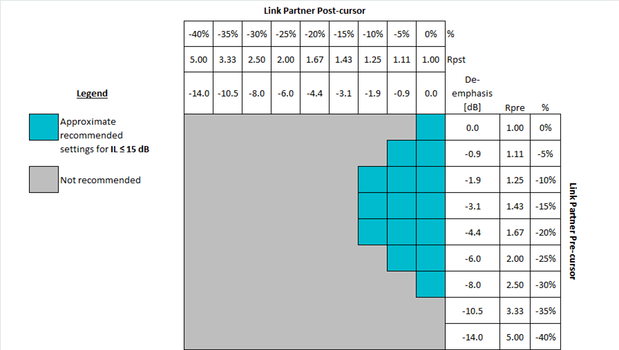
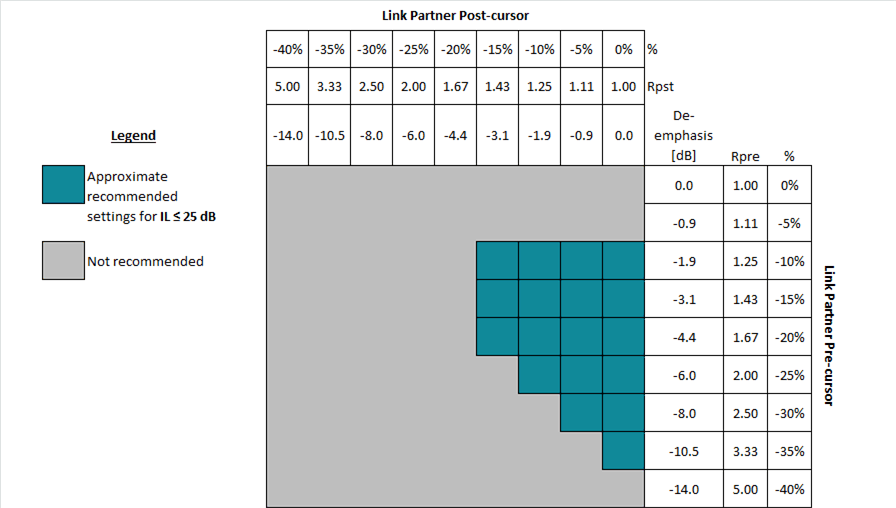
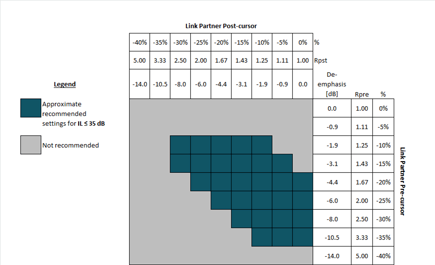
The recommended pre-cursor and post-cursor settings for a given channel will depend on the channel characteristics (mainly insertion loss) as well as the equalization capabilities of the downstream receiver. The DS280DF810 receiver, with its highly-capable CTLE and DFE, does not require a significant amount of pre-cursor or post-cursor. The figures below give general recommendations for pre- and post-cursor for different channel loss conditions. The insertion loss (IL) in these plots refers to the total loss between the link partner transmitter and the DS280DF810 receiver.
 Figure 6-7 Guideline for Link partner FIR Settings When IL ≤ 15dB
 Figure 6-8 Guideline for Link partner FIR Settings When IL ≤ 25dB
 Figure 6-9 Guideline for Link partner FIR Settings When IL ≤ 35dB