ZHCSKG2B September 2016 – October 2019 DS280BR820
PRODUCTION DATA.
- 1 特性
- 2 应用
- 3 说明
- 4 修订历史记录
- 5 Pin Configuration and Functions
- 6 Specifications
- 7 Detailed Description
- 8 Application and Implementation
- 9 Power Supply Recommendations
- 10Layout
- 11器件和文档支持
8.2.2 Front-Port Applications
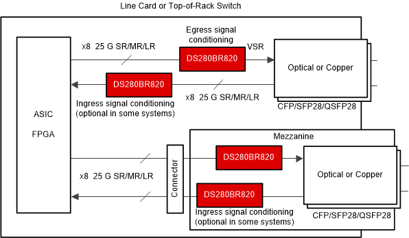
The DS280BR820 has strong equalization capabilities that allow it to equalize insertion loss and extend the reach of front-port channels by 17 dB beyond the normal capabilities of the ASIC while support CAUI-4 and CR4 electrical requirements. The DS280BR820 is designed to apply gain in a linear fashion in order to support longer distances between the switch ASIC and the front-port module. A single DS280BR820 can be used to support all eight egress channels or all eight ingress channels for two 100 GbE ports. Figure 10 illustrates this configuration.
 Figure 10. Typical Front-Port Application Diagram
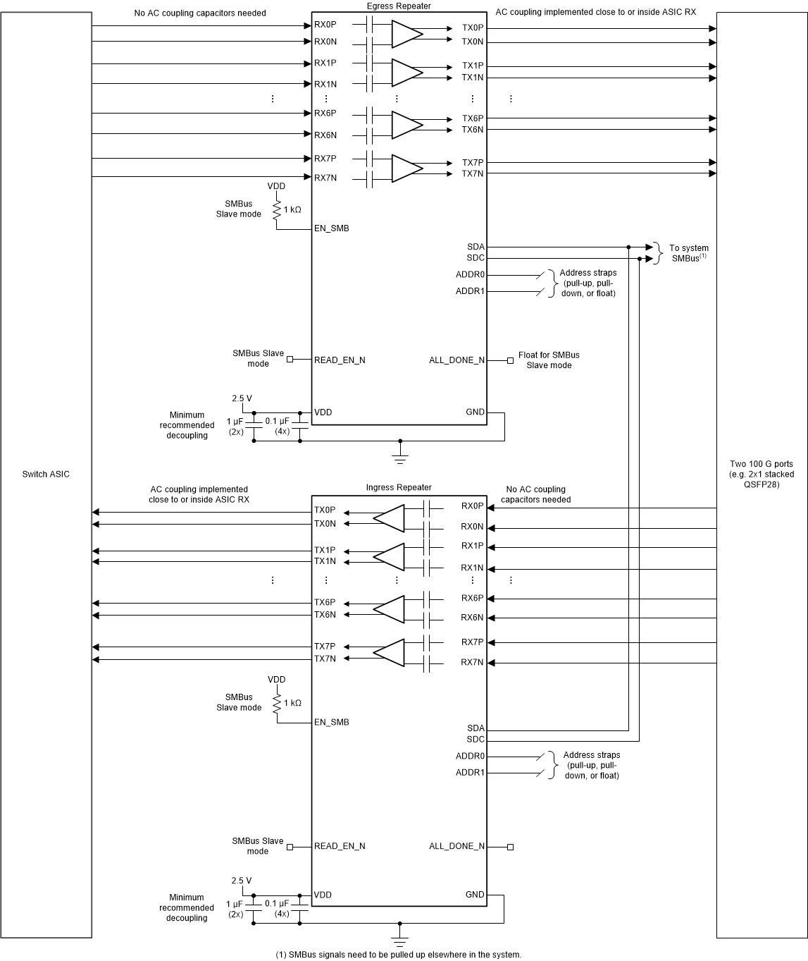
 Standard front-port modules have AC coupling capacitors included inside the module. The DS280BR820, therefore, is ideal for front-port Egress signal conditioning applications since it includes AC coupling capacitors on the input (RX) side and does not include AC coupling capacitors on the output (TX) side.
 Figure 11. DS280BR820 Recommended for Front-port Egress
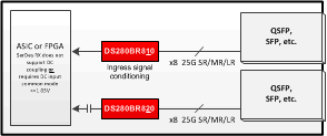
 The optimum solution for front-port Ingress signal conditioning applications depends on whether the ASIC RX supports DC coupling and whether it can support an input common mode voltage of 1.05 V. For further guidance on determining if the ASIC RX supports DC coupling, refer to Figure 7. If the ASIC RX supports DC coupling and can tolerate an input common mode voltage of 1.05 V or less, then the DS280BR820 is the optimum solution for front-port Ingress signal conditioning. If the ASIC RX does not support DC coupling or cannot tolerate an input common mode voltage of 1.05 V, then the pin-compatible DS280BR810 may be the optimum solution.
 Figure 12. DS280BR820 Recommended for Front-port Ingress
  Figure 13. DS280BR820 or DS280BR810 Recommended for Front-port Ingress
  Figure 14. Typical Front-port Schematic