ZHCSME1C August 2018 – June 2021 DS250DF230
PRODUCTION DATA
- 1 特性
- 2 应用
- 3 说明
- 4 Revision History
- 5 说明(续)
- 6 Pin Configuration and Functions
- 7 Specifications
-
8 Detailed Description
- 8.1 Overview
- 8.2 Functional Block Diagram
- 8.3
Feature Description
- 8.3.1 Device Data Path Operation
- 8.3.2 Signal Detect
- 8.3.3 Continuous Time Linear Equalizer (CTLE)
- 8.3.4 Variable Gain Amplifier (VGA)
- 8.3.5 Cross-Point Switch
- 8.3.6 Decision Feedback Equalizer (DFE)
- 8.3.7 Clock and Data Recovery (CDR)
- 8.3.8 Calibration Clock
- 8.3.9 Differential Driver With FIR Filter
- 8.3.10 Debug Features
- 8.3.11 Interrupt Signals
- 8.4 Device Functional Modes
- 8.5 Programming
- 8.6 Register Maps
- 9 Application and Implementation
- 10Power Supply Recommendations
- 11Layout
- 12Device and Documentation Support
- 13Electrostatic Discharge Caution
- 14术语表
- 15Mechanical, Packaging, and Orderable Information
封装选项
机械数据 (封装 | 引脚)
散热焊盘机械数据 (封装 | 引脚)
- RTV|32
订购信息
8.3.10.3 Eye-Opening Monitor
The DS250DF230’s Eye-Opening Monitor (EOM) measures the internal data eye at the input of the decision slicer and can be used for 2 functions:
- Horizontal Eye Opening (HEO) and Vertical Eye Opening (VEO) measurement
- Full Eye Diagram Capture
The HEO measurement is made at the 0 V crossing and is read in channel register 0x27. The VEO measurement is made at the 0.5 UI mark and is read in channel register 0x28. The HEO and VEO registers can be read from channel registers 0x27 and 0x28 at any time while the CDR is locked. The following equations are used to convert the contents of channel registers 0x27 and 0x28 into their appropriate units:
- HEO [UI] = Reg_0x27 ÷ 32
- VEO [mV] = Reg_0x28 × 3.125
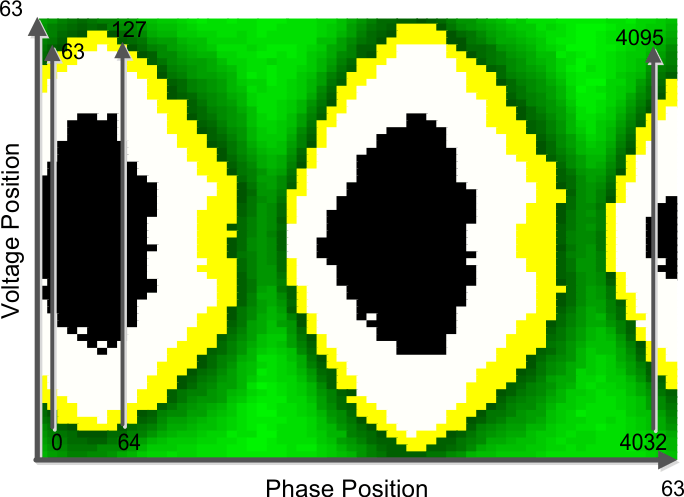
A full eye diagram capture can be performed when the CDR is locked. The eye diagram is constructed within a 64 × 64 array, where each cell in the matrix consists of an 16-bit word representing the total number of hits recorded at that particular phase and voltage offset. Users can manually adjust the vertical scaling of the EOM or allow the state machine to control the scaling which is the default option. The horizontal scaling controlled by the state machine is always directly proportional to the data rate.
When a full eye diagram plot is captured, the retimer will shift out four 16-bit words of residual data that must be discarded followed by 4096 16-bit words that make up the 64 × 64 eye plot. The first actual word of the eye plot from the retimer is for (X, Y) position (0,0), which is the earliest position in time and the most negative position in voltage. Each time the eye plot data is read out, the voltage position is incremented. Once the voltage position has incremented to position 63 (the most positive voltage), the next read will cause the voltage position to reset to 0 (the most negative voltage) and the phase position to increment. This process will continue until the entire 64 × 64 matrix is read out. Figure 8-8 shows the EOM read out sequence overlaid on top of a simple eye opening plot. In this plot any hits are shown in green. This type of plot is helpful for quickly visualizing the HEO and VEO. Users can apply different algorithms to the output data to plot density or color gradients to the output data.
 Figure 8-8 EOM Full Eye
Capture Readout
Figure 8-8 EOM Full Eye
Capture ReadoutTo manually control the EOM vertical range, remove scaling control from the state machine then select the desired range:
Channel Reg 0x2C[6] → 0 (see Table 8-3).
| CH REG 0x11[7:6] VALUE | EOM VERTICAL RANGE [mV] |
|---|---|
| 2’b00 | ±100 |
| 2'b01 | ±200 |
| 2'b10 | ±300 |
| 2'b11 | ±400 |
The EOM operates as an under-sampled circuit. This allows the EOM to be useful in identifying over equalization, ringing and other gross signal conditioning issues. However, the EOM cannot be correlated to a bit error rate.
The EOM can be accessed in two ways to read out the entire eye plot:
- Multi-byte reads can be used such that data is repeatedly latched out from channel register 0x25.
- With single byte reads, the MSB are located in register 0x25 and the LSB are located in register 0x26. In this mode, the device must be addressed each time a new byte is read.
To perform a full eye capture with the EOM, follow the steps listed in Table 8-4 within the desired channel register set:
| STEP | REGISTER [bits] | Operation | VALUE | DESCRIPTION |
|---|---|---|---|---|
| 1 | 0x67[5] | Write | 0 | Disable lock EOM lock monitoring |
| 2 | 0x2C[6] | Write | 0 | Set the desired EOM vertical range |
| 0x11[7:6] | Write | 2'b-- | ||
| 3 | 0x11[5] | Write | 0 | Power on the EOM |
| 4 | 0x24[7] | Write | 1 | Enable fast EOM |
| 5 | 0x24[0] 0x25 0x26 | Read | 1 | Begin read out of the 64 × 64 array, discard first 4 words Ch reg 0x24[0] is self-clearing. |
| 0x25 is the MSB of the 16-bit word | ||||
| 0x26 is the LSB of the 16-bit word | ||||
| 6 | 0x25 | Read | Continue reading information until the 64 × 64 array is complete. | |
| 0x26 | ||||
| 7 | 0x67[5] | Write | 1 | Return the EOM to its original state. Undo steps 1-4 |
| 0x2C[6] | Write | 1 | ||
| 0x11[5] | Write | 1 | ||
| 0x24[7] | Write | 0 |