ZHCSME1C August 2018 – June 2021 DS250DF230
PRODUCTION DATA
- 1 特性
- 2 应用
- 3 说明
- 4 Revision History
- 5 说明(续)
- 6 Pin Configuration and Functions
- 7 Specifications
-
8 Detailed Description
- 8.1 Overview
- 8.2 Functional Block Diagram
- 8.3
Feature Description
- 8.3.1 Device Data Path Operation
- 8.3.2 Signal Detect
- 8.3.3 Continuous Time Linear Equalizer (CTLE)
- 8.3.4 Variable Gain Amplifier (VGA)
- 8.3.5 Cross-Point Switch
- 8.3.6 Decision Feedback Equalizer (DFE)
- 8.3.7 Clock and Data Recovery (CDR)
- 8.3.8 Calibration Clock
- 8.3.9 Differential Driver With FIR Filter
- 8.3.10 Debug Features
- 8.3.11 Interrupt Signals
- 8.4 Device Functional Modes
- 8.5 Programming
- 8.6 Register Maps
- 9 Application and Implementation
- 10Power Supply Recommendations
- 11Layout
- 12Device and Documentation Support
- 13Electrostatic Discharge Caution
- 14术语表
- 15Mechanical, Packaging, and Orderable Information
封装选项
机械数据 (封装 | 引脚)
散热焊盘机械数据 (封装 | 引脚)
- RTV|32
订购信息
9.2.3 Backplane and Mid-Plane Applications
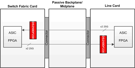
The DS250DF230 has strong equalization capabilities that allow it to recover data over channels up to 35-dB insertion loss. As a result, the optimum placement for the DS250DF230 in a backplane/mid-plane application is with the higher-loss channel segment at the input and the lower-loss channel segment at the output. This reduces the equalization burden on the downstream ASIC/FPGA, as the DS250DF230 is equalizing a majority of the overall channel. This type of asymmetric placement is not a requirement, but when an asymmetric placement is required due to the presence of a passive backplane or mid-plane, then this becomes the recommended placement.
 Figure 9-10 Backplane/Mid-Plane Application Block Diagram
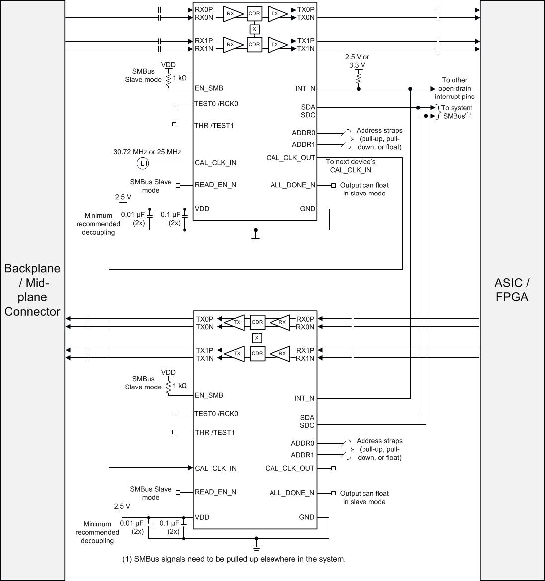
 Figure 9-11 Backplane/Mid-Plane Application Schematic