ZHCSJ76A March   2018  – April 2019 DRV8343-Q1

PRODUCTION DATA.  

  1. 特性
  2. 应用
  3. 说明
    1.     简化原理图
  4. 修订历史记录
  5. Device Comparison Table
  6. Pin Configuration and Functions
    1.     Pin Functions—DRV8343H
    2.     Pin Functions—DRV8343S
  7. Specifications
    1. 7.1 Absolute Maximum Ratings
    2. 7.2 ESD Ratings
    3. 7.3 Recommended Operating Conditions
    4. 7.4 Thermal Information
    5. 7.5 Electrical Characteristics
    6. 7.6 SPI Timing Requirements
    7. 7.7 Typical Characteristics
  8. Detailed Description
    1. 8.1 Overview
    2. 8.2 Functional Block Diagram
    3. 8.3 Feature Description
      1. 8.3.1 Three Phase Smart Gate Drivers
        1. 8.3.1.1 PWM Control Modes
          1. 8.3.1.1.1 6x PWM Mode (PWM_MODE = 000b or MODE Pin Tied to AGND)
          2. 8.3.1.1.2 3x PWM Mode (PWM_MODE = 001b or MODE Pin = 18 kΩ to AGND)
          3. 8.3.1.1.3 1x PWM Mode (PWM_MODE = 010b or MODE Pin = 75 kΩ to AGND)
          4. 8.3.1.1.4 Independent Half-Bridge PWM Mode (PWM_MODE = 011b or MODE Pin is > 1.5 MΩ to AGND or Hi-Z)
          5. 8.3.1.1.5 Phases A and B are Independent Half-Bridges, Phase C is Independent FET (MODE = 100b)
          6. 8.3.1.1.6 Phases B and C are Independent Half-Bridges, Phase A is Independent FET (MODE = 101b or MODE Pin is 75 kΩ to DVDD)
          7. 8.3.1.1.7 Phases A is Independent Half-Bridge, Phases B and C are Independent FET (MODE = 110b or MODE Pin is 18 kΩ to DVDD)
          8. 8.3.1.1.8 Independent MOSFET Drive Mode (PWM_MODE = 111b or MODE Pin = 0.47 kΩ to DVDD)
        2. 8.3.1.2 Device Interface Modes
          1. 8.3.1.2.1 Serial Peripheral Interface (SPI)
          2. 8.3.1.2.2 Hardware Interface
        3. 8.3.1.3 Gate Driver Voltage Supplies
        4. 8.3.1.4 Smart Gate Drive Architecture
          1. 8.3.1.4.1 IDRIVE: MOSFET Slew-Rate Control
          2. 8.3.1.4.2 TDRIVE: MOSFET Gate Drive Control
          3. 8.3.1.4.3 Propagation Delay
          4. 8.3.1.4.4 MOSFET VDS Monitors
          5. 8.3.1.4.5 VDRAIN Sense Pin
          6. 8.3.1.4.6 nFAULT Pin
      2. 8.3.2 DVDD Linear Voltage Regulator
      3. 8.3.3 Pin Diagrams
      4. 8.3.4 Low-Side Current Sense Amplifiers
        1. 8.3.4.1 Bidirectional Current Sense Operation
        2. 8.3.4.2 Unidirectional Current Sense Operation (SPI only)
        3. 8.3.4.3 Amplifier Calibration Modes
        4. 8.3.4.4 MOSFET VDS Sense Mode (SPI Only)
      5. 8.3.5 Gate Driver Protective Circuits
        1. 8.3.5.1  VM Supply Undervoltage Lockout (UVLO)
        2. 8.3.5.2  VCP Charge Pump Undervoltage Lockout (CPUV)
        3. 8.3.5.3  MOSFET VDS Overcurrent Protection (VDS_OCP)
          1. 8.3.5.3.1 VDS Latched Shutdown (OCP_MODE = 00b)
          2. 8.3.5.3.2 VDS Automatic Retry (OCP_MODE = 01b)
          3. 8.3.5.3.3 VDS Report Only (OCP_MODE = 10b)
          4. 8.3.5.3.4 VDS Disabled (OCP_MODE = 11b)
        4. 8.3.5.4  VSENSE Overcurrent Protection (SEN_OCP)
          1. 8.3.5.4.1 VSENSE Latched Shutdown (OCP_MODE = 00b)
          2. 8.3.5.4.2 VSENSE Automatic Retry (OCP_MODE = 01b)
          3. 8.3.5.4.3 VSENSE Report Only (OCP_MODE = 10b)
          4. 8.3.5.4.4 VSENSE Disabled (OCP_MODE = 11b)
        5. 8.3.5.5  Gate Driver Fault (GDF)
        6. 8.3.5.6  Thermal Warning (OTW)
        7. 8.3.5.7  Thermal Shutdown (OTSD)
          1. 8.3.5.7.1 Latched Shutdown (OTSD_MODE = 0b)
          2. 8.3.5.7.2 Automatic Recovery (OTSD_MODE = 1b)
        8. 8.3.5.8  Open Load Detection (OLD)
          1. 8.3.5.8.1 Open Load Detection in Passive Mode (OLP)
            1. 8.3.5.8.1.1 OLP Steps
          2. 8.3.5.8.2 Open Load Detection in Active Mode (OLA)
        9. 8.3.5.9  Offline Shorts Diagnostics
          1. 8.3.5.9.1 Offline Short-to-Supply Diagnostic (SHT_BAT)
          2. 8.3.5.9.2 Offline Short-to-Ground Diagnostic (SHT_GND)
        10. 8.3.5.10 Reverse Supply Protection
    4. 8.4 Device Functional Modes
      1. 8.4.1 Gate Driver Functional Modes
        1. 8.4.1.1 Sleep Mode
        2. 8.4.1.2 Operating Mode
        3. 8.4.1.3 Fault Reset (CLR_FLT or ENABLE Reset Pulse)
    5. 8.5 Programming
      1. 8.5.1 SPI Communication
        1. 8.5.1.1 SPI
          1. 8.5.1.1.1 SPI Format
    6. 8.6 Register Maps
      1. 8.6.1 Status Registers
        1. 8.6.1.1 FAULT Status Register (Address = 0x00) [reset = 0x00]
          1. Table 16. FAULT Status Register Field Descriptions
        2. 8.6.1.2 DIAG Status A Register (Address = 0x01) [reset = 0x00]
          1. Table 17. DIAG Status A Register Field Descriptions
        3. 8.6.1.3 DIAG Status B Register (Address = 0x02) [reset = 0x00]
          1. Table 18. DIAG Status B Register Field Descriptions
        4. 8.6.1.4 DIAG Status C Register (address = 0x03) [reset = 0x00]
          1. Table 19. DIAG Status C Register Field Descriptions
      2. 8.6.2 Control Registers
        1. 8.6.2.1  IC1 Control Register (Address = 0x04) [reset = 0x00]
          1. Table 21. IC1 Control Field Descriptions
        2. 8.6.2.2  IC2 Control Register (address = 0x05) [reset = 0x40]
          1. Table 22. IC2 Control Field Descriptions
        3. 8.6.2.3  IC3 Control Register (Address = 0x06) [reset = 0xFF]
          1. Table 23. IC3 Control Field Descriptions
        4. 8.6.2.4  IC4 Control Register (Address = 0x07) [reset = 0xFF]
          1. Table 24. IC4 Control Field Descriptions
        5. 8.6.2.5  IC5 Control Register (Address = 0x08) [reset = 0xFF]
          1. Table 25. IC5 Control Field Descriptions
        6. 8.6.2.6  IC6 Control Register (Address = 0x09) [reset = 0x99]
          1. Table 26. IC6 Control Field Descriptions
        7. 8.6.2.7  IC7 Control Register (Address = 0x0A) [reset = 0x99]
          1. Table 27. IC7 Control Field Descriptions
        8. 8.6.2.8  IC8 Control Register (Address = 0x0B) [reset = 0x99]
          1. Table 28. IC8 Control Field Descriptions
        9. 8.6.2.9  IC9 Control Register (Address = 0x0C) [reset = 0x2F]
          1. Table 29. IC9 Control Field Descriptions
        10. 8.6.2.10 IC10 Control Register (Address = 0x0D) [reset = 0x61]
          1. Table 30. IC10 Control Field Descriptions
        11. 8.6.2.11 IC11 Control Register (Address = 0x0E) [reset = 0x00]
          1. Table 31. IC11 Control Field Descriptions
        12. 8.6.2.12 IC12 Control Register (Address = 0x0F) [reset = 0x2A]
          1. Table 32. IC12 Control Field Descriptions
        13. 8.6.2.13 IC13 Control Register (Address = 0x10) [reset = 0x7F]
          1. Table 33. IC13 Control Field Descriptions
        14. 8.6.2.14 IC14 Control Register (Address = 0x10) [reset = 0x00]
          1. Table 34. IC14 Control Field Descriptions
  9. Application and Implementation
    1. 9.1 Application Information
    2. 9.2 Typical Application
      1. 9.2.1 Primary Application
        1. 9.2.1.1 Design Requirements
        2. 9.2.1.2 Detailed Design Procedure
          1. 9.2.1.2.1 External MOSFET Support
            1. 9.2.1.2.1.1 Example
          2. 9.2.1.2.2 IDRIVE Configuration
            1. 9.2.1.2.2.1 Example
          3. 9.2.1.2.3 VDS Overcurrent Monitor Configuration
            1. 9.2.1.2.3.1 Example
          4. 9.2.1.2.4 Sense Amplifier Bidirectional Configuration
            1. 9.2.1.2.4.1 Example
          5. 9.2.1.2.5 External Components
        3. 9.2.1.3 Application Curves
      2. 9.2.2 Application With One Sense Amplifier
        1. 9.2.2.1 Design Requirements
        2. 9.2.2.2 Detailed Design Procedure
          1. 9.2.2.2.1 Sense Amplifier Unidirectional Configuration
            1. 9.2.2.2.1.1 Example
            2. 9.2.2.2.1.2 Unused pins
          2. 9.2.2.2.2 External Components
  10. 10Power Supply Recommendations
    1. 10.1 Power Supply Consideration in Generator Mode
    2. 10.2 Bulk Capacitance Sizing
  11. 11Layout
    1. 11.1 Layout Guidelines
    2. 11.2 Layout Example
  12. 12器件和文档支持
    1. 12.1 器件支持
      1. 12.1.1 器件命名规则
    2. 12.2 文档支持
      1. 12.2.1 相关文档
    3. 12.3 接收文档更新通知
    4. 12.4 社区资源
    5. 12.5 商标
    6. 12.6 静电放电警告
    7. 12.7 术语表
  13. 13机械、封装和可订购信息

封装选项

机械数据 (封装 | 引脚)
散热焊盘机械数据 (封装 | 引脚)
订购信息

Independent MOSFET Drive Mode (PWM_MODE = 111b or MODE Pin = 0.47 kΩ to DVDD)

In independent MOSFET drive mode, the INHx and INLx pins control the outputs, GHx and GLx, respectively. This control mode lets the DRV8343-Q1 device drive separate high-side and low-side loads with each half-bridge. These types of loads include unidirectional brushed DC motors, solenoids, and low-side and high-side switches. In this mode, turning on both the high-side and low-side MOSFETs at the same time in a given half-bridge gate driver is possible to use the device as a high-side or low-side driver. The dead time (tDEAD) is bypassed in the mode and must be inserted by the external MCU.

Table 7. Independent PWM Mode Truth Table

INLx INHx GLx GHx
0 0 L L
0 1 L H
1 0 H L
1 1 H H

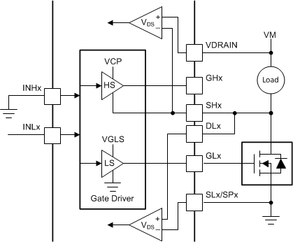
Figure 12 shows how the DRV8343-Q1 device can be used to connect a high-side load and a low-side load at the same time with one half-bridge and drive the loads independently. In this mode, the VDS monitors are active for both the MOSFETs to protect from an overcurrent condition.
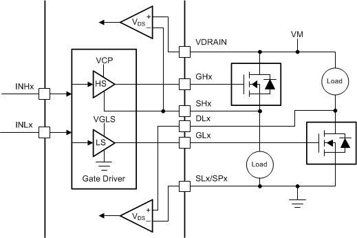
DRV8343-Q1 drv8323-q1-independent-pwm-high-side-and-low-side-drivers.gifFigure 12. Independent PWM High-Side and Low-Side Drivers

If the half-bridge is used to implement only a high-side or low-side driver, using the VDS monitors to help protect from an overcurrent condition is possible as shown in Figure 13 or Figure 14. The unused gate driver can stay disconnected.
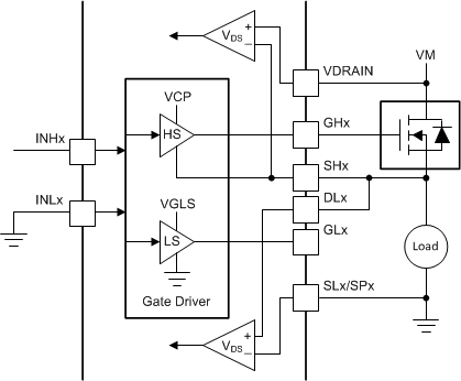
DRV8343-Q1 drv8323-q1-single-high-side-driver.gifFigure 13. One High-Side Driver
DRV8343-Q1 drv8323-q1-single-low-side-driver.gifFigure 14. One Low-Side Driver

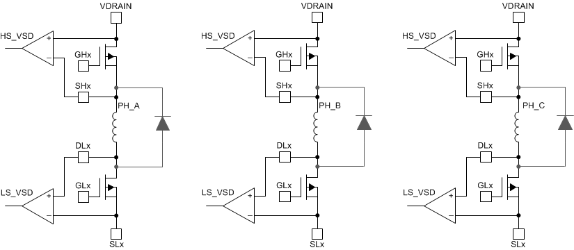
Figure 15 shows how the DRV8343-Q1 device can be used to connect a solenoid load where both the high-side and low-side MOSFETs can be turned on at the same time to drive the load without causing shoot-through. TI recommends having the external diodes for current recirculation. If a half-bridge is not used, the gate pins (GHx and GLx) can stay unconnected and the sense pins (SHx and DLx) can be tied directly or with a resistor to GND.
DRV8343-Q1 drv8343-q1-solenoid-drive-configuration.gifFigure 15. Solenoid Drive Configuration