ZHCSQ30 December   2022 DRV8317

PRODUCTION DATA  

  1.   1
  2. 特性
  3. 应用
  4. 说明
  5. Revision History
  6. Device Comparison Table
  7. Pin Configuration and Functions
  8. Specifications
    1. 7.1 Absolute Maximum Ratings
    2. 7.2 ESD Ratings
    3. 7.3 Recommended Operating Conditions
    4. 7.4 Thermal Information
    5. 7.5 Electrical Characteristics
  9. Detailed Description
    1. 8.1 Overview
    2. 8.2 Functional Block Diagram
    3. 8.3 Feature Description
      1. 8.3.1  Output Stage
      2. 8.3.2  Control Modes
        1. 8.3.2.1 6x PWM Mode
        2. 8.3.2.2 3x PWM Mode
      3. 8.3.3  Device Interface Modes
        1. 8.3.3.1 Serial Peripheral Interface (SPI)
        2. 8.3.3.2 Hardware Interface
      4. 8.3.4  AVDD Linear Voltage Regulator
      5. 8.3.5  Charge Pump
      6. 8.3.6  Slew Rate Control
      7. 8.3.7  Cross Conduction (Dead Time)
      8. 8.3.8  Propagation Delay
      9. 8.3.9  Pin Diagrams
        1. 8.3.9.1 Logic Level Input Pin (Internal Pulldown)
        2. 8.3.9.2 Logic Level Input Pin (Internal Pullup)
        3. 8.3.9.3 Open Drain Pin
        4. 8.3.9.4 Push Pull Pin
        5. 8.3.9.5 Four Level Input Pin
      10. 8.3.10 Current Sense Amplifiers
        1. 8.3.10.1 Current Sense Amplifier Operation
      11. 8.3.11 Protections
        1. 8.3.11.1 Under Voltage Protection (UVP)
        2. 8.3.11.2 VM Under Voltage Warn (VMUV_WARN) Protection
          1. 8.3.11.2.1 VM Under Voltage Warn Automatic Retry (VMUV_WARN_MODE = 00b or 01b)
          2. 8.3.11.2.2 VM Under Voltage Warn Report Only (VMUV_WARN_MODE = 10b)
          3. 8.3.11.2.3 VM Under Voltage Warn Disabled (VMUV_WARN_MODE = 11b)
        3. 8.3.11.3 Over Current Protection (OCP)
          1. 8.3.11.3.1 OCP Latched Fault (OCP_MODE = 010b)
          2. 8.3.11.3.2 OCP Automatic Retry (OCP_MODE = 000b or 001b)
          3. 8.3.11.3.3 OCP Report Only (OCP_MODE = 011b)
        4. 8.3.11.4 VM Over Voltage Protection (OVP)
        5. 8.3.11.5 SPI Fault
        6. 8.3.11.6 System (OTP Read) Fault
        7. 8.3.11.7 Thermal Protection
          1. 8.3.11.7.1 FET Over Temperature Warning (OTW_FET)
          2. 8.3.11.7.2 FET Over Temperature Shutdown (OTS_FET)
          3. 8.3.11.7.3 LDO Over Temperature Shutdown
    4. 8.4 Device Functional Modes
      1. 8.4.1 Functional Modes
        1. 8.4.1.1 Sleep Mode
        2. 8.4.1.2 Operating Mode
        3. 8.4.1.3 Fault Reset (FLT_CLR or nSLEEP Reset Pulse)
    5. 8.5 SPI Communication
      1. 8.5.1 Programming
        1. 8.5.1.1 SPI Format
    6. 8.6 DRV8317 Registers
  10. Application and Implementation
    1. 9.1 Application Information
    2. 9.2 Typical Applications
      1. 9.2.1 Three-Phase Brushless-DC Motor Control
        1. 9.2.1.1 Detailed Design Procedure
          1. 9.2.1.1.1 Motor Voltage
        2. 9.2.1.2 Driver Propagation Delay and Dead Time
        3. 9.2.1.3 Delay Compensation
        4. 9.2.1.4 Current Sensing and Output Filtering
        5. 9.2.1.5 Application Curves
    3. 9.3 Alternate Applications
  11. 10Power Supply Recommendations
    1. 10.1 Bulk Capacitance
  12. 11Layout
    1. 11.1 Layout Guidelines
    2. 11.2 Layout Example
    3. 11.3 Thermal Considerations
      1. 11.3.1 Power Dissipation and Junction Temperature Estimation
  13. 12Device and Documentation Support
    1. 12.1 支持资源
    2. 12.2 Trademarks
    3. 12.3 静电放电警告
    4. 12.4 术语表
  14. 13Mechanical, Packaging, and Orderable Information

封装选项

机械数据 (封装 | 引脚)
散热焊盘机械数据 (封装 | 引脚)
订购信息

Slew Rate Control

An adjustable gate-drive current to the MOSFETs allows for driver output slew rate control. The MOSFET VDS slew rate is a critical factor in optimizing radiated emissions, energy and duration of diode recovery spikes and switching voltage transients related to parasitics. This slew rate is predominantly determined by the rate of gate charge to the MOSFETs as shown in Figure 8-9.

GUID-8432E314-2438-40AC-A7C4-9FFC7B91C27D-low.svg Figure 8-9 Slew Rate Control

The slew rate of each half-bridge can be adjusted by SLEW pin in hardware variant or by SLEW_RATE register in SPI variant. The slew rate is calculated by the rise-time and fall-time of the voltage on OUTx pin as shown in Figure 8-10.
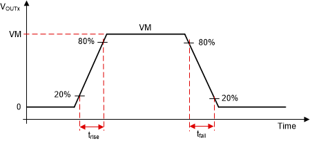
GUID-F5D59AE7-CBEF-4515-9170-0C199CA0FABF-low.gif Figure 8-10 Slew Rate Measurement