ZHCSBP4C September   2013  – December 2016 DRV8303

PRODUCTION DATA.  

  1. 特性
  2. 应用
  3. 说明
  4. 修订历史记录
  5. Pin Configuration and Functions
  6. Specifications
    1. 6.1 Absolute Maximum Ratings
    2. 6.2 ESD Ratings
    3. 6.3 Recommended Operating Conditions
    4. 6.4 Thermal Information
    5. 6.5 Electrical Characteristics
    6. 6.6 Current Shunt Amplifier Characteristics
    7. 6.7 SPI Characteristics (Slave Mode Only)
    8. 6.8 Gate Timing and Protection Switching Characteristics
    9. 6.9 Typical Characteristics
  7. Detailed Description
    1. 7.1 Overview
    2. 7.2 Functional Block Diagram
    3. 7.3 Feature Description
      1. 7.3.1 Three-Phase Gate Driver
      2. 7.3.2 Current Shunt Amplifiers
      3. 7.3.3 Protection Features
        1. 7.3.3.1 Power Stage Protection
        2. 7.3.3.2 Overcurrent Protection (OCP) and Reporting
        3. 7.3.3.3 Undervoltage Protection (UVLO)
        4. 7.3.3.4 Overvoltage Protection (GVDD_OV)
        5. 7.3.3.5 Overtemperature Protection
        6. 7.3.3.6 Fault and Protection Handling
      4. 7.3.4 Start-Up and Shutdown Sequence Control
    4. 7.4 Device Functional Modes
      1. 7.4.1 EN_GATE
      2. 7.4.2 DTC
      3. 7.4.3 VDD_SPI
      4. 7.4.4 DC_CAL
    5. 7.5 Programming
      1. 7.5.1 SPI Communication
        1. 7.5.1.1 SPI
        2. 7.5.1.2 SPI Format
    6. 7.6 Register Maps
      1. 7.6.1 Read / Write Bit
      2. 7.6.2 Address Bits
      3. 7.6.3 SPI Data Bits
        1. 7.6.3.1 Status Registers
        2. 7.6.3.2 Control Registers
        3. 7.6.3.3 Overcurrent Adjustment
  8. Application and Implementation
    1. 8.1 Application Information
      1. 8.1.1 Gate Driver Power-Up Sequencing Errata
    2. 8.2 Typical Application
      1. 8.2.1 Design Requirements
      2. 8.2.2 Detailed Design Procedure
        1. 8.2.2.1 Gate Drive Average Current Load
        2. 8.2.2.2 Overcurrent Protection Setup
        3. 8.2.2.3 Sense Amplifier Setup
      3. 8.2.3 Application Curves
  9. Power Supply Recommendations
    1. 9.1 Bulk Capacitance
  10. 10Layout
    1. 10.1 Layout Guidelines
    2. 10.2 Layout Example
  11. 11器件和文档支持
    1. 11.1 文档支持
      1. 11.1.1 相关文档
    2. 11.2 接收文档更新通知
    3. 11.3 社区资源
    4. 11.4 商标
    5. 11.5 静电放电警告
    6. 11.6 Glossary
  12. 12机械、封装和可订购信息

封装选项

机械数据 (封装 | 引脚)
散热焊盘机械数据 (封装 | 引脚)
订购信息

Layout

Layout Guidelines

Use these layout recommendations when designing a PCB for the DRV8303.

  • The DRV8303 makes an electrical connection to GND through the PowerPAD. Always check to ensure that the PowerPAD has been properly soldered (see PowerPAD™ Thermally Enhanced Package).
  • PVDD bypass capacitors should be placed close to their corresponding pins with a low impedance path to device GND (PowerPAD).
  • GVDD bypass capacitor should be placed close its corresponding pin with a low impedance path to device GND (PowerPAD).
  • AVDD and DVDD bypass capacitors should be placed close to their corresponding pins with a low impedance path to the AGND pin. It is preferable to make this connection on the same layer.
  • AGND should be tied to device GND (PowerPAD) through a low impedance trace/copper fill.
  • Add stitching vias to reduce the impedance of the GND path from the top to bottom side.
  • Try to clear the space around and underneath the DRV8303 to allow for better heat spreading from the PowerPAD.

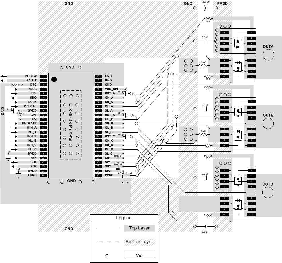
Layout Example

DRV8303 Schem_02_SLOS846.png Figure 13. Layout Recommendation