ZHCSE90D September   2015  – September 2020 DLPC910

PRODUCTION DATA  

  1. 特性
  2. 应用
  3. 说明
  4. Revision History
  5. Pin Configuration and Functions
    1.     Pin Functions
  6. Specifications
    1. 6.1 Absolute Maximum Ratings
    2. 6.2 ESD Ratings
    3. 6.3 Recommended Operating Conditions
    4. 6.4 Thermal Information
    5. 6.5 Electrical Characteristics
    6. 6.6 Timing Requirements
  7. Detailed Description
    1. 7.1 Overview
    2. 7.2 Functional Block Diagram
    3. 7.3 Feature Description
      1. 7.3.1  Input LVDS Interface
      2. 7.3.2  Data Clock
      3. 7.3.3  Data Valid
      4. 7.3.4  Interface Training
      5. 7.3.5  Row and Block Interface
        1. 7.3.5.1 Row Mode
        2. 7.3.5.2 Block Mode
      6. 7.3.6  Control Interface
        1. 7.3.6.1 Complement Data
        2. 7.3.6.2 North South Flip
        3. 7.3.6.3 Watchdog
        4. 7.3.6.4 DMD Mirror Float
        5. 7.3.6.5 Load4
          1. 7.3.6.5.1 Load4 Row Addressing
          2. 7.3.6.5.2 Load4 Block Clears
      7. 7.3.7  Status Interface
        1. 7.3.7.1 ECP2 Finished
        2. 7.3.7.2 Initialization Active
        3. 7.3.7.3 Reset Active
        4. 7.3.7.4 DMD_TYPE
        5. 7.3.7.5 DDC_Version(2:0)
        6. 7.3.7.6 DMD_IRQ
        7. 7.3.7.7 LED Indicators
          1. 7.3.7.7.1 VLED0
          2. 7.3.7.7.2 VLED1
      8. 7.3.8  Reset and System Clock
        1. 7.3.8.1 Controller Reset
        2. 7.3.8.2 Main Oscillator Clock
      9. 7.3.9  I2C Interface
        1. 7.3.9.1 Configuration Pins
        2. 7.3.9.2 Communications Interface
          1. 7.3.9.2.1 Command Format
      10. 7.3.10 DMD Interface
        1. 7.3.10.1 DDC_DOUT
        2. 7.3.10.2 DDC_SCTRL
        3. 7.3.10.3 DDC_DCLKOUT
        4. 7.3.10.4 DMD Reset Interface
          1. 7.3.10.4.1 Mirror Reset Control
        5. 7.3.10.5 Enable and Interrupt Signals
        6. 7.3.10.6 Serial Control Port
      11. 7.3.11 Flash PROM Interface
        1. 7.3.11.1 JTAG Interface
        2. 7.3.11.2 PGM Interface
    4. 7.4 Device Functional Modes
      1. 7.4.1 DMD Row Operation
        1. 7.4.1.1 Data and Command Write Cycle
      2. 7.4.2 Block Mode Operation
      3. 7.4.3 Block Clear
      4. 7.4.4 Mirror Clocking Pulse
      5. 7.4.5 DMD Array Subset
      6. 7.4.6 Global Mirror Clocking Pulse Consideration
    5. 7.5 Register Map
      1. 7.5.1 Register Table Overview
        1. 7.5.1.1  DESTOP_INTERRUPT Register
        2. 7.5.1.2  MAIN_STATUS Register
        3. 7.5.1.3  DESTOP_CAL Register
        4. 7.5.1.4  DESTOP_DMD_ID_REG Register
        5. 7.5.1.5  DESTOP_CATBITS_REG Register
        6. 7.5.1.6  DESTOP_VERSION Register
        7. 7.5.1.7  DESTOP_RESET_REG Register
        8. 7.5.1.8  DESTOP_INFIFO_STATUS Register
        9. 7.5.1.9  DESTOP_BUS_SWAP Register
        10. 7.5.1.10 DESTOP_DMDCTRL Register
        11. 7.5.1.11 DESTOP_BIT_FLIP Register
  8. Application and Implementation
    1. 8.1 Application Information
    2. 8.2 Typical Application
      1. 8.2.1 High Speed Lithography Application
        1. 8.2.1.1 Design Requirements
        2. 8.2.1.2 Detailed Design Procedure
        3. 8.2.1.3 Application Curves
  9. Power Supply Recommendations
    1. 9.1 Power Supply Distribution and Requirements
    2. 9.2 Power Down Requirements
  10. 10Layout
    1. 10.1 Layout Guidelines
      1. 10.1.1 PCB Design Standards
      2. 10.1.2 Signal Layers
      3. 10.1.3 General PCB Routing
        1. 10.1.3.1 Trace Minimum Spacing
        2. 10.1.3.2 Trace Widths and Lengths
          1. 10.1.3.2.1 LVDS Output Bus Skew
        3. 10.1.3.3 Trace Impedance and Routing Priority
      4. 10.1.4 Power and Ground Planes
      5. 10.1.5 Power Vias
      6. 10.1.6 Decoupling
      7. 10.1.7 Flex Connector Plating
    2. 10.2 Layout Example
  11. 11Device and Documentation Support
    1. 11.1 Device Support
      1. 11.1.1 Device Nomenclature
      2. 11.1.2 Device Markings
    2. 11.2 Documentation Support
      1. 11.2.1 Related Documentation
    3. 11.3 支持资源
    4. 11.4 Trademarks
    5. 11.5 静电放电警告
    6. 11.6 术语表
  12. 12Mechanical, Packaging, and Orderable Information

封装选项

机械数据 (封装 | 引脚)
散热焊盘机械数据 (封装 | 引脚)
订购信息

Interface Training

The DLPC910 detects the phase differences between the ½ speed clock (used in the device driving the LVDS data) and the internally generated ½ speed data clocks to select a clock phase for data capture. This is done by supplying a simple repeating pattern on all of the data inputs while the INIT_ACTIVE output of the DLPC910 is high/active. The details of the training pattern are described below.

Figure 7-1 shows a simple block diagram of the training pattern insertion logic.
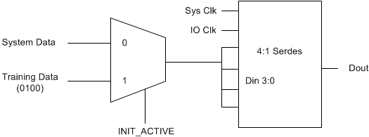
GUID-DBB0E26C-1A59-444A-A40D-51200025C84A-low.gifFigure 7-1 Block Diagram of Training Pattern Logic

The expected training pattern is 0100. In Figure 7-2, the data input to the 4:1 SERDES cells is captured on the rising edge of the ½ speed system clock. The output latency shown is based on the documentation for the Xilinx SERDES cells. Individual implementation may vary depending on the type of cells, technology, and design technique used.
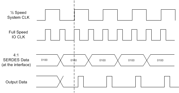
GUID-035B0C52-978A-48B5-9830-C655B16C6909-low.gifFigure 7-2 Training Pattern Alignment
Note:

In Xilinx FPGAs (due to the construction of the ISERDES and OSERDES cells) a pattern of 0010 needs to be applied to the output/transmitting SERDES cells data pins (D1 = 0, D2 = 0, D3 = 1, D4 = 0) in order to receive a result of 0100 (Q1 = 0, Q2 = 1, Q3 = 0, Q4 = 0) at the input/receiving SERDES cell.

The patterns should be applied on all of the data and DVALID pins. In this respect, the interface is treated as a 17 bit interface with DVALID being the 17th data bit. The receiving logic in the DLPC910 adjusts the clock phase until the correct pattern is seen at the inputs. This allows DLPC910 to correctly select a clock phase for data capture and will contribute to a more robust interface. It is important that the training pattern is applied to the DVALID and data inputs of the DLPC910 before reset to the device is de-asserted, as training commences immediately on the de-assertion of reset. The INIT_ACTIVE signal is asserted while the device is held in reset in order to help facilitate this behavior.