ZHCSAV5F April   2013  – May 2019 DLPC350

PRODUCTION DATA.  

  1. 特性
  2. 应用
  3. 说明
    1.     简化应用
  4. 修订历史记录
  5. Pin Configuration and Functions
    1.     Pin Functions
    2. Table 1. Power and Ground Pin Descriptions
  6. Specifications
    1. 6.1  Absolute Maximum Ratings
    2. 6.2  ESD Ratings
    3. 6.3  Recommended Operating Conditions
    4. 6.4  Thermal Information
    5. 6.5  I/O Electrical Characteristics
    6. 6.6  I2C0 and I2C1 Interface Timing Requirements
    7. 6.7  Port 1 Input Pixel Interface Timing Requirements
    8. 6.8  Port 2 Input Pixel Interface (FPD-Link Compatible LVDS Input) Timing Requirements
    9. 6.9  System Oscillator Timing Requirements
    10. 6.10 Reset Timing Requirements
    11. 6.11 Video Timing Input Blanking Specification
      1. 6.11.1 Source Input Blanking
    12. 6.12 Programmable Output Clocks Switching Characteristics
    13. 6.13 DMD Interface Switching Characteristics
    14. 6.14 JTAG Interface: I/O Boundary Scan Application Switching Characteristics
  7. Parameter Measurement Information
    1. 7.1 Power Consumption
  8. Detailed Description
    1. 8.1 Overview
    2. 8.2 Functional Block Diagram
    3. 8.3 Feature Description
      1. 8.3.1 Board Level Test Support
    4. 8.4 Device Functional Modes
      1. 8.4.1 Structured Light Applications
      2. 8.4.2 (LVDS) Receiver Supported Pixel Mapping Modes
  9. Application and Implementation
    1. 9.1 Application Information
    2. 9.2 Typical Applications
      1. 9.2.1 Typical Chipset Application
        1. 9.2.1.1 Design Requirements
        2. 9.2.1.2 Detailed Design Procedure
          1. 9.2.1.2.1 DLPC350 System Interfaces
            1. 9.2.1.2.1.1 Control Interface
            2. 9.2.1.2.1.2 Input Data Interface
          2. 9.2.1.2.2 DLPC350 System Output Interfaces
            1. 9.2.1.2.2.1 Illumination Interface
            2. 9.2.1.2.2.2 Trigger Interface (Sync Outputs)
          3. 9.2.1.2.3 DLPC350 System Support Interfaces
            1. 9.2.1.2.3.1 Reference Clock
            2. 9.2.1.2.3.2 PLL
            3. 9.2.1.2.3.3 Program Memory Flash Interface
          4. 9.2.1.2.4 DMD Interfaces
            1. 9.2.1.2.4.1 DLPC350 to DMD Digital Data
            2. 9.2.1.2.4.2 DLPC350 to DMD Control Interface
            3. 9.2.1.2.4.3 DLPC350 to DMD Micromirror Reset Control Interface
  10. 10Power Supply Recommendations
    1. 10.1 System Power and Reset
      1. 10.1.1 Default Conditions
        1. 10.1.1.1 1.2-V System Power
        2. 10.1.1.2 1.8-V System Power
        3. 10.1.1.3 1.9-V System Power
        4. 10.1.1.4 3.3-V System Power
        5. 10.1.1.5 FPD-Link Input LVDS System Power
      2. 10.1.2 System Power-up and Power-down Sequence
      3. 10.1.3 Power-On Sense (POSENSE) Support
      4. 10.1.4 Power-Good (PWRGOOD) Support
      5. 10.1.5 5-V Tolerant Support
      6. 10.1.6 Power Reset Operation
      7. 10.1.7 System Reset Operation
  11. 11Layout
    1. 11.1 Layout Guidelines
      1. 11.1.1 DMD Interface Design Considerations
      2. 11.1.2 DMD Termination Requirements
      3. 11.1.3 Decoupling Capacitors
      4. 11.1.4 Power Plane Recommendations
      5. 11.1.5 Signal Layer Recommendations
      6. 11.1.6 General Handling Guidelines for CMOS-Type Pins
      7. 11.1.7 PCB Manufacturing
        1. 11.1.7.1 General Guidelines
        2. 11.1.7.2 Trace Widths and Minimum Spacings
        3. 11.1.7.3 Routing Constraints
        4. 11.1.7.4 Fiducials
        5. 11.1.7.5 Flex Considerations
        6. 11.1.7.6 DLPC350 Thermal Considerations
    2. 11.2 Layout Example
      1. 11.2.1 Printed Circuit Board Layer Stackup Geometry
      2. 11.2.2 Recommended DLPC350 MOSC Crystal Oscillator Configuration
      3. 11.2.3 Recommended DLPC350 PLL Layout Configuration
  12. 12器件和文档支持
    1. 12.1 器件支持
      1. 12.1.1 视频时序参数定义
      2. 12.1.2 器件命名规则
      3. 12.1.3 器件标记
    2. 12.2 文档支持
      1. 12.2.1 相关文档
    3. 12.3 商标
    4. 12.4 Glossary
  13. 13机械、封装和可订购信息
    1. 13.1 Package Option Addendum
      1. 13.1.1 Packaging Information

封装选项

机械数据 (封装 | 引脚)
散热焊盘机械数据 (封装 | 引脚)

Source Input Blanking

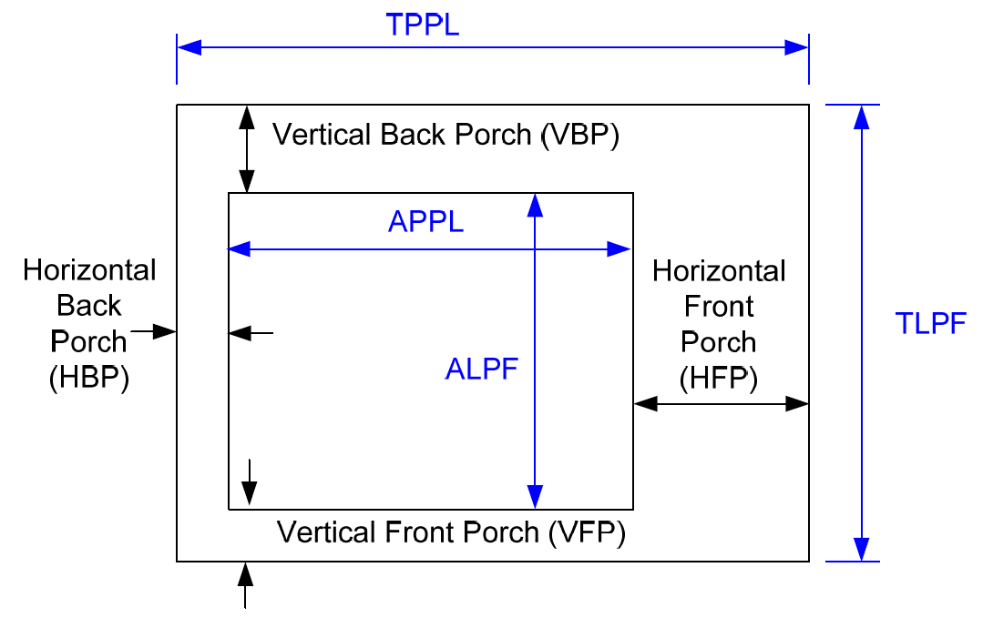
The vertical and horizontal blanking requirements for both input ports are defined in Table 3, except when using a 120 Hz source. In this case, please use the source input blanking timing found in Table 4. Refer to the video timing parameter definitions listed in视频时序参数定义. Also, see Figure 7 for Parallel I/F Frame Timing.

Table 3. Source Input Blanking Requirements

PORT PARAMETER MINIMUM BLANKING
Port 1 Vertical Blanking VBP (tp_vbp) 370 µs
VFP (tp_vfp) 2 lines
Total vertical blanking 370 µs + 3 lines
VSYNC high (tp_vsw) 1 line
Port 2 Vertical Blanking VBP (tp_vbp) 370 µs
VFP (tp_vfp) 0 lines
Total vertical blanking 370 µs + 3 lines
VSYNC high (tp_vsw) 1 line
Port 1 and 2 Horizontal Blanking HBP (tp_hbp) 10 pixels
HFP (tp_hfp) 0 pixels
Total horizontal blanking for 0.45 WXGA DMD 154286 ÷ Source APPL pixels (round up)
HSYNC high (tp_hsw) 16 pixels

Table 4. 120 Hz Source Input Blanking Timings on Port 1
PORT PARAMETER MINIMUM BLANKING
Vertical Blanking VBP (tp_vbp) 3 lines
VFP (tp_vfp) 17 lines
Total vertical blanking 30 lines
VSYNC high (tp_vsw) 10 lines
Horizontal Blanking HBP (tp_hbp) 10 pixels
HFP (tp_hfp) 56 pixels
Total horizontal blanking 128 pixels
HSYNC high (tp_vsw) 64 pixels
Pixel Clock 146.0 MHz
DLPC350 Porch_DLPS029.pngFigure 6. Horizontal and Vertical Blanking Diagram
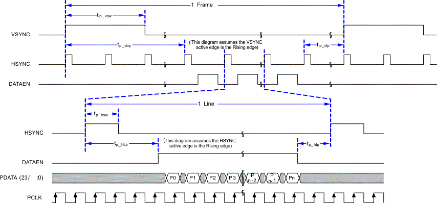
DLPC350 Pll_frame.pngFigure 7. Parallel I/F Frame Timing