ZHCSDJ3C March 2015 – June 2019 DLPC150
PRODUCTION DATA.
- 1 特性
- 2 应用
- 3 说明
- 4 修订历史记录
- 5 Pin Configuration and Functions
-
6 Specifications
- 6.1 Absolute Maximum Ratings
- 6.2 ESD Ratings
- 6.3 Recommended Operating Conditions
- 6.4 Thermal Information
- 6.5 Electrical Characteristics Over Recommended Operating Conditions
- 6.6 Electrical Characteristics
- 6.7 High-Speed Sub-LVDS Electrical Characteristics
- 6.8 Low-Speed SDR Electrical Characteristics
- 6.9 System Oscillators Timing Requirements
- 6.10 Power-Up and Reset Timing Requirements
- 6.11 Parallel Interface Frame Timing Requirements
- 6.12 Parallel Interface General Timing Requirements
- 6.13 Flash Interface Timing Requirements
- 7 Parameter Measurement Information
- 8 Detailed Description
- 9 Application and Implementation
- 10Power Supply Recommendations
-
11Layout
- 11.1
Layout Guidelines
- 11.1.1 PCB Layout Guidelines For Internal Controller PLL Power
- 11.1.2 DLPC150 Reference Clock
- 11.1.3 General PCB Recommendations
- 11.1.4 General Handling Guidelines for Unused CMOS-Type Pins
- 11.1.5 Maximum Pin-to-Pin, PCB Interconnects Etch Lengths
- 11.1.6 Number of Layer Changes
- 11.1.7 Stubs
- 11.1.8 Terminations
- 11.1.9 Routing Vias
- 11.2 Layout Example
- 11.3 Thermal Considerations
- 11.1
Layout Guidelines
- 12器件和文档支持
- 13"机械、封装和可订购信息
11.1.2 DLPC150 Reference Clock
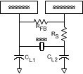
The DLPC150 requires an external reference clock to feed its internal PLL. A crystal or oscillator can supply this reference. For flexibility, the DLPC150 accepts either of two reference clock frequencies (see Table 12), but both must have a maximum frequency variation of ±200 ppm (including aging, temperature, and trim component variation). When a crystal is used, several discrete components are also required as shown in Figure 18.

A. CL = Crystal load capacitance (farads)
B. CL1 = 2 × (CL – Cstray_pll_refclk_i)
C. CL2 = 2 × (CL – Cstray_pll_refclk_o)
D. Where: Cstray_pll_refclk_i = Sum of package and PCB stray capacitance at the crystal pin associated with the controller pin pll_refclk_i. Cstray_pll_refclk_o = Sum of package and PCB stray capacitance at the crystal pin associated with the controller pin pll_refclk_o.
Figure 18. Recommended Crystal Oscillator Configuration