ZHCSIA7 May 2018 DLPA4000
PRODUCTION DATA.
- 1 特性
- 2 应用
- 3 说明
- 4 修订历史记录
- 5 Pin Configuration and Functions
- 6 Specifications
-
7 Detailed Description
- 7.1 Overview
- 7.2 Functional Block Description
- 7.3
Feature Description
- 7.3.1 Supply and Monitoring
- 7.3.2 Illumination
- 7.3.3 External Power MOSFET Selection
- 7.3.4 DMD Supplies
- 7.3.5 Buck Converters
- 7.3.6 Auxiliary LDOs
- 7.3.7 Measurement System
- 7.4 Device Functional Modes
- 7.5 Programming
- 7.6 Register Maps
- 8 Application and Implementation
- 9 Power Supply Recommendations
- 10Layout
- 11器件和文档支持
- 12机械、封装和可订购信息
10.1.1.1 PowerBlock Gate Control Isolation
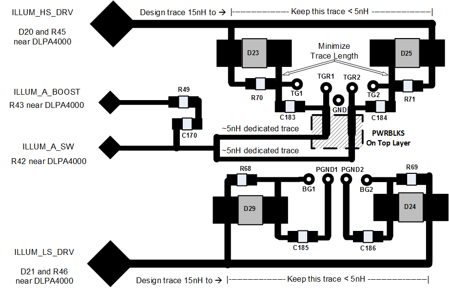
 Figure 26. DLPA4000 Illumination Bottom Layout
 The two power blocks Synchronous Buck NexFET™ Power Block MOSFET Pair in the reference design connects Q11 and Q12 in parallel. This design feature reduces current loss and power loss in the application. Place the two power blocks close to each other. Implement the gate control isolation topologies in the reference design to prevent feedback and ringing on the gate control line from the DLPA4000.
Place a single-shared ILLUM_HS_DRV trace from the PMIC to the two separate gate filtering and isolation component sets (D23, R70, and C183) and (D25, R71, and C184). Place each set close to the the power block high-side MOSFET pins. Minimize the ILLUM_HS_DRV route length. Minimize coupling to other routes. Terminate the ILLUM_HS_DRV from the PMIC in a T-junction. Make sure this termination is very close to the power blocks. Minimize the route beyond the T-junction that goes between the two filter and isolation component sets. Make sure the routing inductance is 5 nH or less on the trace between the filter and isolation sets.
Place D23, R70, and C183 very close together and underneath Q11 with the goal of minimizing the net connecting D23, R70, C183, and the high-side MOSFET pin (Q11 Pin 3). The high-side MOSFET return pin (Q11 Pin 4) requires an independent 5-nH trace before merging with the Top Gate Return of Q12. Make sure that the merged Top Gate Return trace has an inductance of 15 nH on the return to the R-C filter (C170 and R49) near the DLPA4000 device. The isolation components near the Top Gate pin of Q12 (D25, R71, and C184) must follow the same requirements as those isolating Q11 (D23, R70, and C183). The inductance of the high-side illumination driver net connecting D25 to D23 must maintain a value below 5 nH. The high-side MOSFET return pin (Q12 pin 4) requires a 5-nH independent trace before merging with the Q11 Top Gate Return path back to the RC filter.
Route a single-shared ILLUM_LS_DRV trace from the PMIC to the two separate gate filtering and isolation component sets (D29, R68, and C185) and (D24, R69, and C186). Place each component set close to the power block low-side MOSSFET pins. Minimize the ILLUM_LS_DRV route length. Minimize coupling the ILLUM_LS_DRV route to other routes. Terminate the ILLUM_LS_DRV from the PMIC in a T-junction. Make sure this termination is very close to the power blocks. Minimize the route beyond the T-junction that goes between the two filter and isolation component sets. Make sure the routing inductance is 5 nH or less on the trace between the filter and isolation sets)
Make sure the inductance of the trace from D21 and R46 to D29 is as close to 15 nH as possible. Place D29, C185, and R68 directly underneath Q11 to minimize trace impedance. Similarly, place D24, C186, and R69 underneath and as close as possible to Q12. Make sure the inductance of the trace connecting D24 to D29 is less than 15 nH.