ZHCSIA7 May 2018 DLPA4000
PRODUCTION DATA.
- 1 特性
- 2 应用
- 3 说明
- 4 修订历史记录
- 5 Pin Configuration and Functions
- 6 Specifications
-
7 Detailed Description
- 7.1 Overview
- 7.2 Functional Block Description
- 7.3
Feature Description
- 7.3.1 Supply and Monitoring
- 7.3.2 Illumination
- 7.3.3 External Power MOSFET Selection
- 7.3.4 DMD Supplies
- 7.3.5 Buck Converters
- 7.3.6 Auxiliary LDOs
- 7.3.7 Measurement System
- 7.4 Device Functional Modes
- 7.5 Programming
- 7.6 Register Maps
- 8 Application and Implementation
- 9 Power Supply Recommendations
- 10Layout
- 11器件和文档支持
- 12机械、封装和可订购信息
10.1 Layout Guidelines
Make sure to consider high peak currents and high switching frequencies when designing the layout to avoid instability and EMI problems.
- Use wide and short traces for high-current paths and for high-current return power ground paths.
- Place, the input capacitor, output capacitor, and the inductor of the DMD HV regulator as close as possible to the DLPA4000 device.
- Separate the ground traces and connect them together at a central point undermeath the device package. This design minimizes ground noise coupling between different buck converters
- The recommended value for the DMD capacitors is 1 µF for VRST and VOFS, 470 nF for VBIAS. The inductor value is 10 µH.
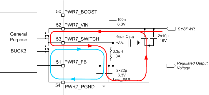
The currents of the buck converters are highest near pins VIN, SWITCH and PGND (). The voltage at the pins VIN, PGND and FB are DC voltages. the SWITCH pin voltage a value betweent eh value of the VIN viltage and teh PGND voltage. The red line in Figure 25 indicates the current flow when the MOSFET between pin 52 and pin 53 is closed. The blue line indicates the current flow when the MOSFET between pin 53 and pin 54 is closed.
The buck converter paths carry the highest currents. Make sure the buck converter paths are as short as possible.
For the LDO DMD, it is recommended to use a 1-µF, 16-V capacitor on the input and a 10-µF, 6.3-V capacitor on the output of the LDO assuming a battery voltage of 12 V.
For LDO bucks, it is recommended to use a 1-µF, 16-V capacitor on the input and a 1-µF, 6.3-V capacitor on the output of the LDO.
 Figure 25. High AC Current Paths in a Buck Converter
 The trace to the VIN pin in this design has high AC currents that prevents voltage drop across the trace. Make sure the trace to the VIN pin has low resistance.
Place the decoupling capacitors as close to the VIN pin as possible.
The SWITCH pin alternates connection to the VIN pin or GND. The SWITCH pin voltage waveform is square with an amplitude equal to VIN. The SWITCH pin voltage containing high frequencies. This situation causes EMI problems unless properly mitigated. Reduce EMI by creating a snubber network (RSN7 and CSN7) Place the resistor and capacitor at the SWITCH pin to prevent or suppress unwanted high-frequency ringing during switching.
The PGND pin sinks high current. Connect the PGND pin to a star ground point so that it does not interfere with other ground connections.
The FB pin is the sense connection for the regulated DC output voltage. No current flows through the FB pin. The device compares the voltage on the FB pin with the internal reference voltage. This comparison controls the loop. Make the FB connection at the load so that the I-R drop does not affect the sensed voltage.