ZHCSBX4D June   2013  – December 2021 DAC7760 , DAC8760

PRODUCTION DATA  

  1. 特性
  2. 应用
  3. 说明
  4. Revision History
  5. Device Comparison Table
  6. Pin Configuration and Functions
  7. Specifications
    1. 7.1  Absolute Maximum Ratings
    2. 7.2  ESD Ratings
    3. 7.3  Recommended Operating Conditions
    4. 7.4  Thermal Information
    5. 7.5  Electrical Characteristics
    6. 7.6  Electrical Characteristics: AC
    7. 7.7  Timing Requirements: Write Mode
    8. 7.8  Timing Requirements: Readback Mode
    9. 7.9  Timing Diagrams
    10. 7.10 Typical Characteristics
  8. Detailed Description
    1. 8.1 Overview
    2. 8.2 Functional Block Diagram
    3. 8.3 Feature Description
      1. 8.3.1  DAC Architecture
      2. 8.3.2  Voltage Output Stage
      3. 8.3.3  Current Output Stage
      4. 8.3.4  Internal Reference
      5. 8.3.5  Digital Power Supply
      6. 8.3.6  DAC Clear
      7. 8.3.7  Power-On Reset
      8. 8.3.8  Alarm Detection
      9. 8.3.9  Watchdog Timer
      10. 8.3.10 Frame Error Checking
      11. 8.3.11 User Calibration
      12. 8.3.12 Programmable Slew Rate
    4. 8.4 Device Functional Modes
      1. 8.4.1 Setting Voltage and Current Output Ranges
      2. 8.4.2 Boost Configuration for IOUT
      3. 8.4.3 Filtering the Current Output (only on the VQFN package)
      4. 8.4.4 HART Interface
        1. 8.4.4.1 For 4-mA to 20-mA Mode
        2. 8.4.4.2 For All Current Output Modes
    5. 8.5 Programming
      1. 8.5.1 Serial Peripheral Interface (SPI)
        1. 8.5.1.1 SPI Shift Register
        2. 8.5.1.2 Write Operation
        3. 8.5.1.3 Read Operation
        4. 8.5.1.4 Stand-Alone Operation
        5. 8.5.1.5 Multiple Devices on the Bus
    6. 8.6 Register Maps
      1. 8.6.1 DACx760 Command and Register Map
        1. 8.6.1.1 DACx760 Register Descriptions
          1. 8.6.1.1.1 Control Register
          2. 8.6.1.1.2 Configuration Register
          3. 8.6.1.1.3 DAC Registers
          4. 8.6.1.1.4 Reset Register
          5. 8.6.1.1.5 Status Register
  9. Application and Implementation
    1. 9.1 Application Information
      1. 9.1.1 Controlling the VOUT and IOUT Pins
        1. 9.1.1.1 VOUT and IOUT Pins are Independent Outputs, Never Simultaneously Enabled
        2. 9.1.1.2 VOUT and IOUT Pins are Independent Outputs, Simultaneously Enabled
        3. 9.1.1.3 VOUT and IOUT Pins are Tied Together, Never Simultaneously Enabled
      2. 9.1.2 Implementing HART in All Current Output Modes
        1. 9.1.2.1 Using CAP2 Pin on VQFN Package
        2. 9.1.2.2 Using the ISET-R Pin
      3. 9.1.3 Short-Circuit Current Limiting
    2. 9.2 Typical Application
      1. 9.2.1 Design Requirements
      2. 9.2.2 Detailed Design Procedure
      3. 9.2.3 Application Curves
  10. 10Power Supply Recommendations
  11. 11Layout
    1. 11.1 Layout Guidelines
      1. 11.1.1 Thermal Considerations
    2. 11.2 Layout Example
  12. 12Device and Documentation Support
    1. 12.1 Documentation Support
      1. 12.1.1 Related Documentation
    2. 12.2 接收文档更新通知
    3. 12.3 支持资源
    4. 12.4 Trademarks
    5. 12.5 Electrostatic Discharge Caution
    6. 12.6 术语表
  13. 13Mechanical, Packaging, and Orderable Information

封装选项

机械数据 (封装 | 引脚)
散热焊盘机械数据 (封装 | 引脚)
订购信息

Power-On Reset

The DACx760 incorporates two internal POR circuits for the DVDD and AVDD supplies. The DVDD and AVDD POR signals are ANDed together so that both supplies must be at their minimal specified values for the device to not be in a reset condition. These POR circuits initialize internal logic and registers as well as set the analog outputs to a known state while the device supplies are ramping. All registers are reset to their default values with the default value of the data register being determined by the CLR-SEL pin. The behavior of IOUT and VOUT is described in their respective sections. Typically the POR function can be ignored as long as the device supplies power up and maintain the specified minimum voltage levels. However, in the case of supply drop or brownout, the DACx760 can have an internal POR reset event or lose digital memory integrity. Figure 8-4 represents the threshold levels for the internal POR for both the DVDD and AVDD supplies.
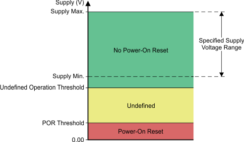
GUID-C4063AB2-BD4E-4CE9-A0BE-F182C4505BAD-low.gifFigure 8-4 Relevant Voltage Levels for POR Circuit

For the DVDD supply, no internal POR occurs for nominal supply operation from 2.7 V (supply minimum) to 5.5 V (supply maximum). For the DVDD supply region between 2.4 V (undefined operation threshold) and 0.8 V (POR threshold), the internal POR circuit may or may not provide a reset over all temperature conditions. For the DVDD supply below 0.8 V (POR threshold), the internal POR resets as long as the supply voltage is below 0.8 V for approximately 1 ms.

For the AVDD supply, no internal POR occurs for nominal supply operation from 10 V (supply minimum) to 36 V (supply maximum). For AVDD supply voltages between 8 V (undefined operation threshold) to 1 V (POR threshold), the internal POR circuit may or may not provide a reset over all temperature conditions. For the AVDD supply below 1 V (POR threshold), the internal POR resets as long as the supply voltage is below 1 V for approximately 1 ms. In case the DVDD or AVDD supply drops to a level where the internal POR signal is indeterminate, either power cycle the device or toggle the LATCH pin followed by a software reset. Both options initialize the internal circuitry to a known state and provide proper operation.