ZHCSBX4D June   2013  – December 2021 DAC7760 , DAC8760

PRODUCTION DATA  

  1. 特性
  2. 应用
  3. 说明
  4. Revision History
  5. Device Comparison Table
  6. Pin Configuration and Functions
  7. Specifications
    1. 7.1  Absolute Maximum Ratings
    2. 7.2  ESD Ratings
    3. 7.3  Recommended Operating Conditions
    4. 7.4  Thermal Information
    5. 7.5  Electrical Characteristics
    6. 7.6  Electrical Characteristics: AC
    7. 7.7  Timing Requirements: Write Mode
    8. 7.8  Timing Requirements: Readback Mode
    9. 7.9  Timing Diagrams
    10. 7.10 Typical Characteristics
  8. Detailed Description
    1. 8.1 Overview
    2. 8.2 Functional Block Diagram
    3. 8.3 Feature Description
      1. 8.3.1  DAC Architecture
      2. 8.3.2  Voltage Output Stage
      3. 8.3.3  Current Output Stage
      4. 8.3.4  Internal Reference
      5. 8.3.5  Digital Power Supply
      6. 8.3.6  DAC Clear
      7. 8.3.7  Power-On Reset
      8. 8.3.8  Alarm Detection
      9. 8.3.9  Watchdog Timer
      10. 8.3.10 Frame Error Checking
      11. 8.3.11 User Calibration
      12. 8.3.12 Programmable Slew Rate
    4. 8.4 Device Functional Modes
      1. 8.4.1 Setting Voltage and Current Output Ranges
      2. 8.4.2 Boost Configuration for IOUT
      3. 8.4.3 Filtering the Current Output (only on the VQFN package)
      4. 8.4.4 HART Interface
        1. 8.4.4.1 For 4-mA to 20-mA Mode
        2. 8.4.4.2 For All Current Output Modes
    5. 8.5 Programming
      1. 8.5.1 Serial Peripheral Interface (SPI)
        1. 8.5.1.1 SPI Shift Register
        2. 8.5.1.2 Write Operation
        3. 8.5.1.3 Read Operation
        4. 8.5.1.4 Stand-Alone Operation
        5. 8.5.1.5 Multiple Devices on the Bus
    6. 8.6 Register Maps
      1. 8.6.1 DACx760 Command and Register Map
        1. 8.6.1.1 DACx760 Register Descriptions
          1. 8.6.1.1.1 Control Register
          2. 8.6.1.1.2 Configuration Register
          3. 8.6.1.1.3 DAC Registers
          4. 8.6.1.1.4 Reset Register
          5. 8.6.1.1.5 Status Register
  9. Application and Implementation
    1. 9.1 Application Information
      1. 9.1.1 Controlling the VOUT and IOUT Pins
        1. 9.1.1.1 VOUT and IOUT Pins are Independent Outputs, Never Simultaneously Enabled
        2. 9.1.1.2 VOUT and IOUT Pins are Independent Outputs, Simultaneously Enabled
        3. 9.1.1.3 VOUT and IOUT Pins are Tied Together, Never Simultaneously Enabled
      2. 9.1.2 Implementing HART in All Current Output Modes
        1. 9.1.2.1 Using CAP2 Pin on VQFN Package
        2. 9.1.2.2 Using the ISET-R Pin
      3. 9.1.3 Short-Circuit Current Limiting
    2. 9.2 Typical Application
      1. 9.2.1 Design Requirements
      2. 9.2.2 Detailed Design Procedure
      3. 9.2.3 Application Curves
  10. 10Power Supply Recommendations
  11. 11Layout
    1. 11.1 Layout Guidelines
      1. 11.1.1 Thermal Considerations
    2. 11.2 Layout Example
  12. 12Device and Documentation Support
    1. 12.1 Documentation Support
      1. 12.1.1 Related Documentation
    2. 12.2 接收文档更新通知
    3. 12.3 支持资源
    4. 12.4 Trademarks
    5. 12.5 Electrostatic Discharge Caution
    6. 12.6 术语表
  13. 13Mechanical, Packaging, and Orderable Information

封装选项

机械数据 (封装 | 引脚)
散热焊盘机械数据 (封装 | 引脚)
订购信息

VOUT and IOUT Pins are Tied Together, Never Simultaneously Enabled

When the VOUT and IOUT pins are tied together, bit 8 of the Configuration Register (DUAL OUTEN) must be set to 0. Bits 2 down to 0 of the Control Register (RANGE) control VOUT and IOUT. Special consideration must be paid to the +VSENSE pin in this case. When VOUT is disabled, the +VSENSE pin is connected to the internal amplifier input through an internal 60-kΩ resistor as shown in Figure 8-2. This internal node has diode clamps to REFIN and GND. Setting bit 6 of the Configuration Register (APD) forces this internal node to be tied to GND through a 10-kΩ resistor, in effect, the +VSENSE pin is tied to GND through a 70-kΩ power-down resistor. Figure 9-1 shows the leakage current into the +VSENSE pin for both settings of the APD bit.
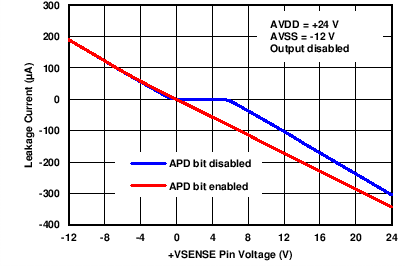
GUID-216033BC-E221-4E03-AD47-FD7E45113AF5-low.pngFigure 9-1 +VSENSE Leakage Current vs Pin Voltage

Whether the APD bit is set or not set, the current output in this case incurs a gain error because the internal resistor acts as a parallel load in addition to the external load. If this gain error is undesirable, it can be corrected through the gain calibration register shown in Table 8-20. Another option is to use the application circuit in Figure 9-2.
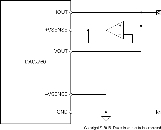
GUID-FF7A3663-1B1A-43C2-A120-2CDBD804F7C6-low.gif Figure 9-2 VOUT and IOUT Tied Together to One Pin

The buffer amplifier prevents leakage through the internal 60-kΩ resistor in current output mode and does not allow it to be seen as a parallel load. The VOUT pin is in high impedance mode in this case and allows minimal leakage current. Note that the offset of the external amplifier adds to the overall VOUT offset error and any potential phase shift from the external amplifier can cause VOUT stability issues.