ZHCSBX4D June   2013  – December 2021 DAC7760 , DAC8760

PRODUCTION DATA  

  1. 特性
  2. 应用
  3. 说明
  4. Revision History
  5. Device Comparison Table
  6. Pin Configuration and Functions
  7. Specifications
    1. 7.1  Absolute Maximum Ratings
    2. 7.2  ESD Ratings
    3. 7.3  Recommended Operating Conditions
    4. 7.4  Thermal Information
    5. 7.5  Electrical Characteristics
    6. 7.6  Electrical Characteristics: AC
    7. 7.7  Timing Requirements: Write Mode
    8. 7.8  Timing Requirements: Readback Mode
    9. 7.9  Timing Diagrams
    10. 7.10 Typical Characteristics
  8. Detailed Description
    1. 8.1 Overview
    2. 8.2 Functional Block Diagram
    3. 8.3 Feature Description
      1. 8.3.1  DAC Architecture
      2. 8.3.2  Voltage Output Stage
      3. 8.3.3  Current Output Stage
      4. 8.3.4  Internal Reference
      5. 8.3.5  Digital Power Supply
      6. 8.3.6  DAC Clear
      7. 8.3.7  Power-On Reset
      8. 8.3.8  Alarm Detection
      9. 8.3.9  Watchdog Timer
      10. 8.3.10 Frame Error Checking
      11. 8.3.11 User Calibration
      12. 8.3.12 Programmable Slew Rate
    4. 8.4 Device Functional Modes
      1. 8.4.1 Setting Voltage and Current Output Ranges
      2. 8.4.2 Boost Configuration for IOUT
      3. 8.4.3 Filtering the Current Output (only on the VQFN package)
      4. 8.4.4 HART Interface
        1. 8.4.4.1 For 4-mA to 20-mA Mode
        2. 8.4.4.2 For All Current Output Modes
    5. 8.5 Programming
      1. 8.5.1 Serial Peripheral Interface (SPI)
        1. 8.5.1.1 SPI Shift Register
        2. 8.5.1.2 Write Operation
        3. 8.5.1.3 Read Operation
        4. 8.5.1.4 Stand-Alone Operation
        5. 8.5.1.5 Multiple Devices on the Bus
    6. 8.6 Register Maps
      1. 8.6.1 DACx760 Command and Register Map
        1. 8.6.1.1 DACx760 Register Descriptions
          1. 8.6.1.1.1 Control Register
          2. 8.6.1.1.2 Configuration Register
          3. 8.6.1.1.3 DAC Registers
          4. 8.6.1.1.4 Reset Register
          5. 8.6.1.1.5 Status Register
  9. Application and Implementation
    1. 9.1 Application Information
      1. 9.1.1 Controlling the VOUT and IOUT Pins
        1. 9.1.1.1 VOUT and IOUT Pins are Independent Outputs, Never Simultaneously Enabled
        2. 9.1.1.2 VOUT and IOUT Pins are Independent Outputs, Simultaneously Enabled
        3. 9.1.1.3 VOUT and IOUT Pins are Tied Together, Never Simultaneously Enabled
      2. 9.1.2 Implementing HART in All Current Output Modes
        1. 9.1.2.1 Using CAP2 Pin on VQFN Package
        2. 9.1.2.2 Using the ISET-R Pin
      3. 9.1.3 Short-Circuit Current Limiting
    2. 9.2 Typical Application
      1. 9.2.1 Design Requirements
      2. 9.2.2 Detailed Design Procedure
      3. 9.2.3 Application Curves
  10. 10Power Supply Recommendations
  11. 11Layout
    1. 11.1 Layout Guidelines
      1. 11.1.1 Thermal Considerations
    2. 11.2 Layout Example
  12. 12Device and Documentation Support
    1. 12.1 Documentation Support
      1. 12.1.1 Related Documentation
    2. 12.2 接收文档更新通知
    3. 12.3 支持资源
    4. 12.4 Trademarks
    5. 12.5 Electrostatic Discharge Caution
    6. 12.6 术语表
  13. 13Mechanical, Packaging, and Orderable Information

封装选项

机械数据 (封装 | 引脚)
散热焊盘机械数据 (封装 | 引脚)
订购信息

Short-Circuit Current Limiting

The DACx760 voltage output includes an internal circuit to typically regulate the load current to about 30 mA. However, this parameter is not production tested or trimmed. Optionally, use an external current limiting circuit on VOUT. However, if the VOUT, IOUT and +VSENSE pins are tied together, this circuit must be placed in the VOUT path before the circuit is tied together to the other pins at the common pin. The nature of the current-limiting circuit depends on the application and load. An example of a unidirectional current limiter is shown in Figure 9-5.
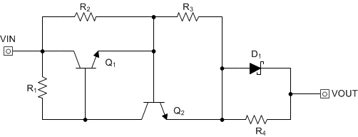
GUID-EDE0E7A1-C2B0-47F9-86B8-1A528B95EF00-low.gifFigure 9-5 Unidirectional Current Limiter Circuit

Under normal operation, most current in this circuit flows through Q1 and into R3. As current increases through R3, so does the voltage drop across R3, which increases the base-emitter voltage of Q2. Eventually the base-emitter voltage of Q2 becomes high enough to turn on Q2, which turns off Q1 and reduce the current that can pass from VIN to VOUT. The value of R3 sets the current limit. Be aware that this example is very simple and only applies for sourcing current into a resistive load. For cases involving both sourcing and sinking current as well as nonresistive loads, more complex circuits are required to achieve bidirectional current limiting.