ZHCSAO1D January   2013  – August 2016 CSD97374Q4M


  1. 特性
  2. 应用
  3. 说明
    1.     Device Images
  4. 修订历史记录
  5. Pin Configuration and Functions
    1.     Pin Functions
  6. Specifications
    1. 6.1 Absolute Maximum Ratings
    2. 6.2 ESD Ratings
    3. 6.3 Recommended Operating Conditions
    4. 6.4 Thermal Information
    5. 6.5 Electrical Characteristics
    6. 6.6 Typical Characteristics
  7. Detailed Description
    1. 7.1 Functional Block Diagram
    2. 7.2 Powering CSD97374Q4M and Gate Drivers
    3. 7.3 Undervoltage Lockout Protection (UVLO)
    4. 7.4 PWM Pin
    5. 7.5 SKIP# Pin
      1. 7.5.1 Zero Crossing (ZX) Operation
    6. 7.6 Integrated Boost-Switch
  8. Application and Implementation
    1. 8.1 Application Information
    2. 8.2 Power Loss Curves
    3. 8.3 Safe Operating Curves (SOA)
    4. 8.4 Normalized Curves
    5. 8.5 Calculating Power Loss and SOA
      1. 8.5.1 Design Example
      2. 8.5.2 Calculating Power Loss
      3. 8.5.3 Calculating SOA Adjustments
  9. Layout
    1. 9.1 Layout Guidelines
      1. 9.1.1 Recommended PCB Design Overview
      2. 9.1.2 Electrical Performance
      3. 9.1.3 Thermal Performance
    2. 9.2 Layout Example
  10. 10器件和文档支持
    1. 10.1 接收文档更新通知
    2. 10.2 社区资源
    3. 10.3 商标
    4. 10.4 静电放电警告
    5. 10.5 Glossary
  11. 11机械封装和可订购信息
    1. 11.1 机械尺寸
    2. 11.2 推荐 PCB 焊盘图案
    3. 11.3 建议模板开口

封装选项

机械数据 (封装 | 引脚)
  • DPC|8
散热焊盘机械数据 (封装 | 引脚)
订购信息

PWM Pin

The PWM pin incorporates an input tri-state function. The device forces the gate driver outputs to low when PWM is driven into the tri-state window and the driver enters a low-power state with zero exit latency. The pin incorporates a weak pullup to maintain the voltage within the tri-state window during low-power modes. Operation into and out of tri-state mode follows the timing diagram outlined in Figure 13.

When VDD reaches the UVLO_H level, a tri-state voltage range (window) is set for the PWM input voltage. The window is defined the PWM voltage range between PWM logic high (VIH) and logic low (VIL) thresholds. The device sets high-level input voltage and low-level input voltage threshold levels to accommodate both 3.3-V (typical) and 5-V (typical) PWM drive signals.

When the PWM exits tri-state, the driver enters CCM for a period of 4 µs, regardless of the state of the SKIP# pin. Normal operation requires this time period in order for the auto-zero comparator to resume.
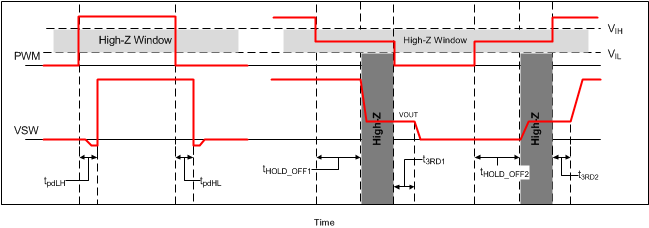
CSD97374Q4M PWM_TriState_Timing_Diagram.gifFigure 13. PWM Tri-State Timing Diagram