ZHCS385D June   2013  – February 2024 CDCE913-Q1 , CDCEL913-Q1

PRODUCTION DATA  

  1.   1
  2. 特性
  3. 应用
  4. 说明
  5. Device Comparison
  6. Pin Configuration and Functions
  7. Specifications
    1. 6.1 Absolute Maximum Ratings
    2. 6.2 ESD Ratings
    3. 6.3 Recommended Operating Conditions
    4. 6.4 Thermal Information
    5. 6.5 Electrical Characteristics
    6. 6.6 Timing Requirements
    7. 6.7 Typical Characteristics
  8. Parameter Measurement Information
  9. Detailed Description
    1. 8.1 Overview
    2. 8.2 Functional Block Diagram
    3. 8.3 Feature Description
      1. 8.3.1 Control Terminal Configuration
      2. 8.3.2 Default Device Configuration
      3. 8.3.3 I2C Serial Interface
      4. 8.3.4 Data Protocol
    4. 8.4 Device Functional Modes
      1. 8.4.1 SDA and SCL Hardware Interface
    5. 8.5 Programming
  10. Application and Implementation
    1. 9.1 Application Information
    2. 9.2 Typical Application
      1. 9.2.1 Design Requirements
      2. 9.2.2 Detailed Design Procedure
        1. 9.2.2.1 Spread-Spectrum Clock (SSC)
        2. 9.2.2.2 PLL Frequency Planning
        3. 9.2.2.3 Crystal Oscillator Start-Up
        4. 9.2.2.4 Frequency Adjustment With Crystal Oscillator Pulling
        5. 9.2.2.5 Unused Inputs and Outputs
        6. 9.2.2.6 Switching Between XO and VCXO Mode
      3. 9.2.3 Application Curves
    3. 9.3 Power Supply Recommendations
    4. 9.4 Layout
      1. 9.4.1 Layout Guidelines
      2. 9.4.2 Layout Example
  11. 10Register Maps
    1. 10.1 I2C Configuration Registers
  12. 11器件和文档支持
    1. 11.1 文档支持
      1. 11.1.1 相关文档
    2. 11.2 接收文档更新通知
    3. 11.3 支持资源
    4. 11.4 商标
    5. 11.5 静电放电警告
    6. 11.6 术语表
  13. 12Revision History
  14. 13Mechanical, Packaging, and Orderable Information

封装选项

机械数据 (封装 | 引脚)
散热焊盘机械数据 (封装 | 引脚)
订购信息

Default Device Configuration

The internal EEPROM of the CDCE913-Q1 and CDCEL913-Q1 devices is preconfigured with a factory default configuration, as shown in Figure 8-1 The input frequency is passed through the output as a default, thus allowing the device to operate in default mode without the extra production step of programming it. The default setting appears after power is supplied or after a power-down–power-up sequence until the device is reprogrammed by the user to a different application configuration. A new register setting is programmed through the serial I2C interface.
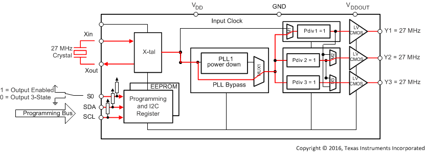
GUID-A843985B-8018-4D1C-8CA8-F02201DC90C5-low.gifFigure 8-1 Default Configuration

Table 8-6 shows the factory default setting for the Control Terminal register. While eight different register settings are possible, in the default configuration, only the first two settings (0 and 1) can be selected with S0, as S1 and S2 are configured as programming pins in default mode.

Table 8-6 Factory Default Setting for Control Terminal Register(1)
Y1PLL1 SETTINGS
EXTERNAL CONTROL PINSOUTPUT
SELECTION
FREQUENCY
SELECTION
SSC
SELECTION
OUTPUT
SELECTION
S2S1S0Y1FS1SSC1Y2Y3
SCL (I2C)SDA (I2C)03-statefVCO1_0OffHi-Z state
SCL (I2C)SDA (I2C)1EnabledfVCO1_0OffEnabled
In default mode or when programmed respectively, S1 and S2 act as serial programming interface, I2C. They do not have any control-pin function but they are internally interpreted as if S1 = 0 and S2 = 0. However, S0 is a control pin, which in the default mode switches all outputs ON or OFF (as previously predefined).