ZHCSJ35C September 2016 – May 2021 CC3220R , CC3220S , CC3220SF
PRODUCTION DATA
- 1 特性
- 2 应用
- 3 说明
- 4 功能方框图
- 5 Revision History
- 6 Device Comparison
- 7 Terminal Configuration and Functions
-
8 Specifications
- 8.1 Absolute Maximum Ratings
- 8.2 ESD Ratings
- 8.3 Power-On Hours (POH)
- 8.4 Recommended Operating Conditions
- 8.5 Current Consumption Summary (CC3220R, CC3220S)
- 8.6 Current Consumption Summary (CC3220SF)
- 8.7 TX Power and IBAT versus TX Power Level Settings
- 8.8 Brownout and Blackout Conditions
- 8.9 Electrical Characteristics (3.3 V, 25°C)
- 8.10 WLAN Receiver Characteristics
- 8.11 WLAN Transmitter Characteristics
- 8.12 WLAN Filter Requirements
- 8.13 Thermal Resistance Characteristics
- 8.14
Timing and Switching Characteristics
- 8.14.1 Power Supply Sequencing
- 8.14.2 Device Reset
- 8.14.3 Reset Timing
- 8.14.4 Wakeup From HIBERNATE Mode
- 8.14.5 Clock Specifications
- 8.14.6
Peripherals Timing
- 8.14.6.1 SPI
- 8.14.6.2 I2S
- 8.14.6.3 GPIOs
- 8.14.6.4 I2C
- 8.14.6.5 IEEE 1149.1 JTAG
- 8.14.6.6 ADC
- 8.14.6.7 Camera Parallel Port
- 8.14.6.8 UART
- 8.14.6.9 SD Host
- 8.14.6.10 Timers
- 9 Detailed Description
- 10Applications, Implementation, and Layout
- 11Device and Documentation Support
- 12Mechanical, Packaging, and Orderable Information
10.1.1 Typical Application —CC3220x Wide-Voltage Mode
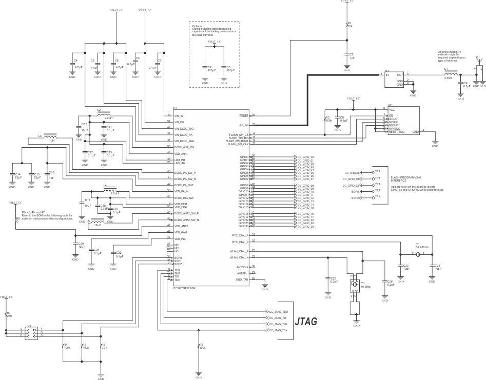
Figure 10-1 shows the schematic for an application using the CC3220x device in the wide-voltage mode of operation. For a full operation reference design, refer to CC3220 SimpleLink™ and Internet of Things Hardware Design Files.
Note:
For complete reference schematics and BOM, see the CC3220x product page.
Table 10-1 lists the bill of materials for an application using the CC3220x device in wide-voltage mode.
 Figure 10-1 CC3220x Wide-Voltage Mode
Application Circuit
Figure 10-1 CC3220x Wide-Voltage Mode
Application CircuitTable 10-1 Bill of Materials for CC3220x in Wide-Voltage Mode
| QUANTITY | DESIGNATOR | VALUE | MANUFACTURER | PART NUMBER | DESCRIPTION |
|---|---|---|---|---|---|
| 1 | C1 | 1 µF | MuRata | GRM155R61A105KE15D | Capacitor, Ceramic, 1 µF, 10 V, ±10%, X5R, 0402 |
| 10 | C2, C6, C10, C12, C13, C14, C19, C20, C22, C23 | 0.1 µF | TDK | C1005X5R1A104K050BA | Capacitor, Ceramic, 0.1 µF, 10 V, ±10%, X5R, 0402 |
| 3 | C3, C4, C5 | 4.7 µF | TDK | C1005X5R0J475M050BC | Capacitor, Ceramic, 4.7 µF, 6.3 V, ±20%, X5R, 0402 |
| 2 | C7, C8 | 100 µF | Taiyo Yuden | LMK325ABJ107MMHT | Capacitor, Ceramic, 100 µF, 10 V, ±20%, X5R, AEC-Q200 Grade 3, 1210 |
| 1 | C9 | 0.5 pF | MuRata | GRM1555C1HR50BA01D | Capacitor, Ceramic, 0.5 pF, 50 V, ±20%, C0G/NP0, 0402 |
| 3 | C11, C18, C21 | 10 µF | MuRata | GRM188R60J106ME47D | Capacitor, Ceramic, 10 µF, 6.3 V, ±20%, X5R, 0603 |
| 1 | C15 | 1 µF | TDK | C1005X5R1A105K050BB | Capacitor, Ceramic, 1 µF, 10 V, ±10%, X5R, 0402 |
| 2 | C16, C17 | 22 µF | TDK | C1608X5R0G226M080AA | Capacitor, Ceramic, 22 µF, 4 V, ±20%, X5R, 0603 |
| 2 | C24, C25 | 10 pF | MuRata | GRM1555C1H100JA01D | Capacitor, Ceramic, 10 pF, 50 V, ±5%, C0G/NP0, 0402 |
| 2 | C26, C27 | 6.2 pF | MuRata | GRM1555C1H6R2CA01D | Capacitor, Ceramic, 6.2 pF, 50 V, ±5%, C0G/NP0, 0402 |
| 1 | E1 | 2.45-GHz Antenna | Taiyo Yuden | AH316M245001-T | ANT Bluetooth W-LAN Zigbee®WiMAX™, SMD |
| 1 | FL1 | 1.02 dB | TDK | DEA202450BT-1294C1-H | Multilayer Chip Band Pass Filter For 2.4 GHz W-LAN/Bluetooth, SMD |
| 1 | L1 | 3.3 nH | MuRata | LQG15HS3N3S02D | Inductor, Multilayer, Air Core, 3.3 nH, 0.3 A, 0.17 ohm, SMD |
| 2 | L2, L4 | 2.2 µH | MuRata | LQM2HPN2R2MG0L | Inductor, Multilayer, Ferrite, 2.2 µH, 1.3 A, 0.08 ohm, SMD |
| 1 | L3 | 1 µH | MuRata | LQM2HPN1R0MG0L | Inductor, Multilayer, Ferrite, 1 µH, 1.6 A, 0.055 ohm, SMD |
| 1 | L5(1) | 10 µH | Taiyo Yuden | CBC2518T100M | Inductor, Wirewound, Ceramic, 10 µH, 0.48 A, 0.36 ohm, SMD |
| 1 | R1 | 10 k | Vishay-Dale | CRCW040210K0JNED | Resistor, 10 k, 5%, 0.063 W, 0402 |
| 4 | R2, R3, R4, R5 | 100 k | Vishay-Dale | CRCW0402100KJNED | Resistor, 100 k, 5%, 0.063 W, 0402 |
| 1 | R6 | 2.7 k | Vishay-Dale | CRCW04022K70JNED | Resistor, 2.7 k, 5%, 0.063 W, 0402 |
| 1 | R7 | 270 | Vishay-Dale | CRCW0402270RJNED | Resistor, 270, 5%, 0.063 W, 0402 |
| 1 | R8(2) | 0 | Panasonic | ERJ-2GE0R00X | Resistor, 0, 5% 0.063W, 0402 |
| 1 | U1 | MX25R | Macronix International Co., LTD | MX25R3235FM1IL0 | Ultra-Low Power, 32-Mbit [x 1/x 2/x 4] CMOS MXSMIO (Serial Multi I/O) Flash Memory, SOP-8 |
| 1 | U2 | CC3220 | Texas Instruments | CC3220SF12RGK | SimpleLink™ Wi-Fi® and internet-of-things Solution, a Single-Chip Wireless MCU, RGK0064B |
| 1 | Y1 | Crystal | Abracon Corportation | ABS07-32.768KHZ-9-T | Crystal, 32.768 KHz, 9PF, SMD |
| 1 | Y2 | Crystal | Epson | Q24FA20H0039600 | Crystal, 40 MHz, 8pF, SMD |
(1) For CC3220SF
device, L5 is populated. For CC3220R and CC3220S devices, L5
is not populated.
(2) For CC3220SF
device, R8 is not populated. For CC3220R and CC3220S devices
if R8 is populated, Pin 47 can be used as GPIO_31.