SWRS045F January   2006  – November 2018 CC1021

PRODUCTION DATA.  

  1. 1Device Overview
    1. 1.1 Features
    2. 1.2 Applications
    3. 1.3 Description
    4. 1.4 Functional Block Diagram
  2. 2Revision History
  3. 3Terminal Configuration and Functions
    1. 3.1 Pin Diagram
    2. 3.2 Pin Configuration
  4. 4Specifications
    1. 4.1  Absolute Maximum Ratings
    2. 4.2  ESD Ratings
    3. 4.3  Recommended Operating Conditions
    4. 4.4  RF Transmit
    5. 4.5  RF Receive
    6. 4.6  RSSI / Carrier Sense
    7. 4.7  Intermediate Frequency (IF)
    8. 4.8  Crystal Oscillator
    9. 4.9  Frequency Synthesizer
    10. 4.10 Digital Inputs / Outputs
    11. 4.11 Current Consumption
    12. 4.12 Thermal Resistance Characteristics for VQFNP Package
  5. 5Detailed Description
    1. 5.1  Overview
    2. 5.2  Functional Block Diagram
    3. 5.3  Configuration Overview
      1. 5.3.1 Configuration Software
    4. 5.4  Microcontroller Interface
      1. 5.4.1 Configuration Interface
      2. 5.4.2 Signal Interface
      3. 5.4.3 PLL Lock Signal
    5. 5.5  4-wire Serial Configuration Interface
    6. 5.6  Signal Interface
      1. 5.6.1 Synchronous NRZ Mode
      2. 5.6.2 Transparent Asynchronous UART Mode
      3. 5.6.3 Synchronous Manchester Encoded Mode
        1. 5.6.3.1 Manchester Encoding and Decoding
    7. 5.7  Data Rate Programming
    8. 5.8  Frequency Programming
      1. 5.8.1 Dithering
    9. 5.9  Receiver
      1. 5.9.1  IF Frequency
      2. 5.9.2  Receiver Channel Filter Bandwidth
      3. 5.9.3  Demodulator, Bit Synchronizer and Data Decision
      4. 5.9.4  Receiver Sensitivity versus Data Rate and Frequency Separation
      5. 5.9.5  RSSI
      6. 5.9.6  Image Rejection Calibration
      7. 5.9.7  Blocking and Selectivity
      8. 5.9.8  Linear IF Chain and AGC Settings
      9. 5.9.9  AGC Settling
      10. 5.9.10 Preamble Length and Sync Word
      11. 5.9.11 Carrier Sense
      12. 5.9.12 Automatic Power-Up Sequencing
      13. 5.9.13 Automatic Frequency Control
      14. 5.9.14 Digital FM
    10. 5.10 Transmitter
      1. 5.10.1 FSK Modulation Formats
      2. 5.10.2 Output Power Programming
      3. 5.10.3 TX Data Latency
      4. 5.10.4 Reducing Spurious Emission and Modulation Bandwidth
    11. 5.11 Input and Output Matching and Filtering
    12. 5.12 Frequency Synthesizer
      1. 5.12.1 VCO, Charge Pump, and PLL Loop Filter
      2. 5.12.2 VCO and PLL Self-Calibration
      3. 5.12.3 PLL Turn-on Time versus Loop Filter Bandwidth
      4. 5.12.4 PLL Lock Time versus Loop Filter Bandwidth
    13. 5.13 VCO and LNA Current Control
    14. 5.14 Power Management
    15. 5.15 On-Off Keying (OOK)
    16. 5.16 Crystal Oscillator
    17. 5.17 Built-in Test Pattern Generator
    18. 5.18 Interrupt on Pin DCLK
      1. 5.18.1 Interrupt Upon PLL Lock
      2. 5.18.2 Interrupt Upon Received Signal Carrier Sense
    19. 5.19 PA_EN and LNA_EN Digital Output Pins
      1. 5.19.1 Interfacing an External LNA or PA
      2. 5.19.2 General-Purpose Output Control Pins
      3. 5.19.3 PA_EN and LNA_EN Pin Drive
    20. 5.20 System Considerations and Guidelines
      1. 5.20.1 SRD Regulations
      2. 5.20.2 Narrowband Systems
      3. 5.20.3 Low Cost Systems
      4. 5.20.4 Battery Operated Systems
      5. 5.20.5 High Reliability Systems
      6. 5.20.6 Frequency Hopping Spread Spectrum Systems (FHSS)
    21. 5.21 Antenna Considerations
    22. 5.22 Configuration Registers
      1. 5.22.1 Memory
  6. 6Applications, Implementation, and Layout
    1. 6.1 Application Information
      1. 6.1.1 Typical Application
    2. 6.2 Design Requirements
      1. 6.2.1 Input / Output Matching
      2. 6.2.2 Bias Resistor
      3. 6.2.3 PLL Loop Filter
      4. 6.2.4 Crystal
      5. 6.2.5 Additional Filtering
      6. 6.2.6 Power Supply Decoupling and Filtering
    3. 6.3 PCB Layout Guidelines
  7. 7Device and Documentation Support
    1. 7.1 Device Support
      1. 7.1.1 Device Nomenclature
    2. 7.2 Documentation Support
      1. 7.2.1 Community Resources
    3. 7.3 Trademarks
    4. 7.4 Electrostatic Discharge Caution
    5. 7.5 Export Control Notice
    6. 7.6 Glossary
  8. 8Mechanical Packaging and Orderable Information
    1. 8.1 Packaging Information

封装选项

机械数据 (封装 | 引脚)
散热焊盘机械数据 (封装 | 引脚)
订购信息

Blocking and Selectivity

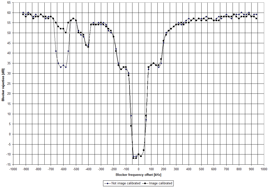
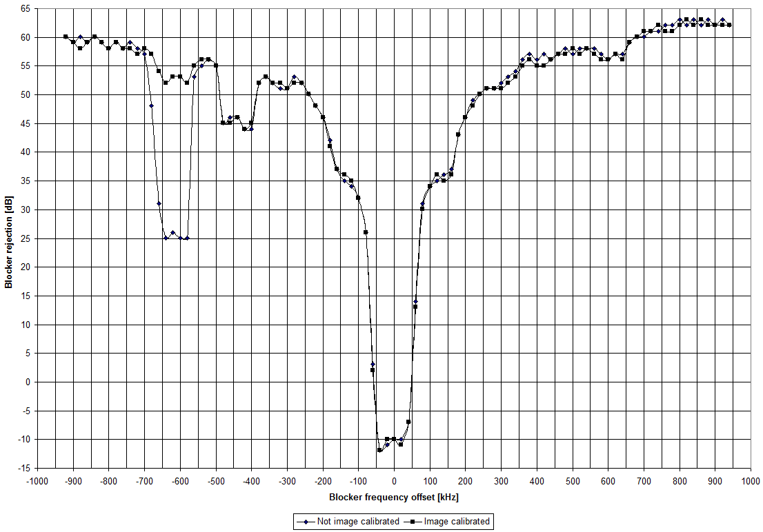
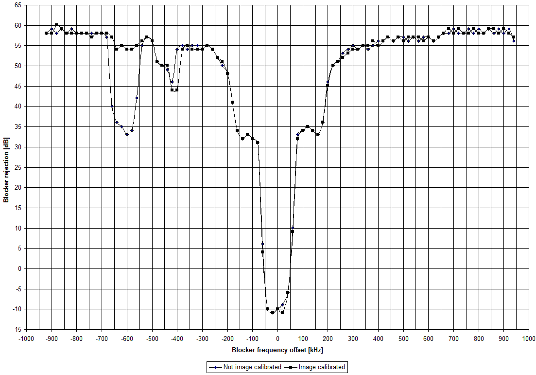
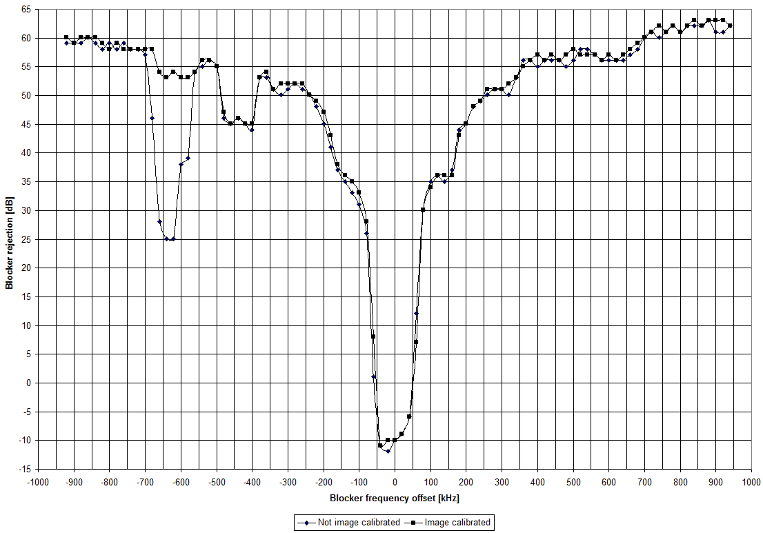
Figure 5-13 shows the blocking/selectivity for 102.4 kHz channel filter bandwidth at 433 MHz and 19.2 kBaud data rate. Figure 5-14 shows the blocking/selectivity for 102.4 kHz channel filter bandwidth at 433 MHz and 38.4 kBaud data rate. Figure 5-15 shows the blocking/selectivity for 102.4 kHz channel filter bandwidth at 868 MHz and 19.2 kBaud data rate. Figure 5-16 shows the blocking/selectivity for 102.4 kHz channel filter bandwidth at 868 MHz and 38.4 kBaud data rate. The blocking rejection is the ratio between a blocker (interferer) and a wanted signal 3 dB above the sensitivity limit.
CC1021 typ_blckr_reject_carrier_freq_434_mhz_19pt2_kbaud_swrs045.png
Figure 5-13 Typical Blocker Rejection. Carrier Frequency Set to 434.3072 MHz (102.4 kHz Channel Filter Bandwidth, 19.2 kBaud)
CC1021 typ_blckr_reject_carrier_freq_868_mhz_19pt2_kbaud_swrs045.png
Figure 5-15 Typical Blocker Rejection. Carrier Frequency Set to 868.3072 MHz (102.4 kHz Channel Filter Bandwidth, 19.2 kBaud)
CC1021 typ_blckr_reject_carrier_freq_434_mhz_38pt4_kbaud_swrs045.png
Figure 5-14 Typical Blocker Rejection. Carrier Frequency Set to 434.3072 MHz (102.4 kHz Channel Filter Bandwidth, 38.4 kBaud)
CC1021 typ_blckr_reject_carrier_freq_868_mhz_38pt4_kbaud_swrs045.png
Figure 5-16 Typical Blocker Rejection. Carrier Frequency Set to 868.3072 MHz (102.4 kHz Channel Filter Bandwidth, 38.4 kBaud)