ZHCSR27D August 2020 – September 2022 BQ79612-Q1 , BQ79614-Q1 , BQ79616-Q1
PRODUCTION DATA
- 1 特性
- 2 应用
- 3 说明
- 4 Revision History
- 5 说明(续)
- 6 Device Comparison Table
- 7 Pin Configuration and Functions
- 8 Specifications
-
9 Detailed Description
- 9.1 Overview
- 9.2 Functional Block Diagram
- 9.3
Feature Description
- 9.3.1 Power Supplies
- 9.3.2 Measurement System
- 9.3.3 Cell Balancing
- 9.3.4 Integrated Hardware Protectors
- 9.3.5 GPIO Configuration
- 9.3.6
Communication, OTP, Diagnostic Control
- 9.3.6.1
Communication
- 9.3.6.1.1 Serial Interface
- 9.3.6.1.2 Daisy Chain Interface
- 9.3.6.1.3 Start Communication
- 9.3.6.1.4 Communication Timeout
- 9.3.6.1.5 Communication Debug Mode
- 9.3.6.1.6 Multidrop Configuration
- 9.3.6.1.7 SPI Master
- 9.3.6.1.8 SPI Loopback
- 9.3.6.2 Fault Handling
- 9.3.6.3 Nonvolatile Memory
- 9.3.6.4 Diagnostic Control/Status
- 9.3.6.1
Communication
- 9.3.7 Bus Bar Support
- 9.4 Device Functional Modes
- 9.5
Register Maps
- 9.5.1 OTP Shadow Register Summary
- 9.5.2 Read/Write Register Summary
- 9.5.3 Read-Only Register Summary
- 9.5.4
Register Field Descriptions
- 9.5.4.1 Device Addressing Setup
- 9.5.4.2 Device ID and Scratch Pad
- 9.5.4.3
General Configuration and Control
- 9.5.4.3.1 DEV_CONF
- 9.5.4.3.2 ACTIVE_CELL
- 9.5.4.3.3 BBVC_POSN1
- 9.5.4.3.4 BBVC_POSN2
- 9.5.4.3.5 PWR_TRANSIT_CONF
- 9.5.4.3.6 COMM_TIMEOUT_CONF
- 9.5.4.3.7 TX_HOLD_OFF
- 9.5.4.3.8 STACK_RESPONSE
- 9.5.4.3.9 BBP_LOC
- 9.5.4.3.10 COMM_CTRL
- 9.5.4.3.11 CONTROL1
- 9.5.4.3.12 CONTROL2
- 9.5.4.3.13 CUST_CRC_HI
- 9.5.4.3.14 CUST_CRC_LO
- 9.5.4.3.15 CUST_CRC_RSLT_HI
- 9.5.4.3.16 CUST_CRC_RSLT_LO
- 9.5.4.4 Operation Status
- 9.5.4.5 ADC Configuration and Control
- 9.5.4.6
ADC Measurement Results
- 9.5.4.6.1 VCELL16_HI/LO
- 9.5.4.6.2 VCELL15_HI/LO
- 9.5.4.6.3 VCELL14_HI/LO
- 9.5.4.6.4 VCELL13_HI/LO
- 9.5.4.6.5 VCELL12_HI/LO
- 9.5.4.6.6 VCELL11_HI/LO
- 9.5.4.6.7 VCELL10_HI/LO
- 9.5.4.6.8 VCELL9_HI/LO
- 9.5.4.6.9 VCELL8_HI/LO
- 9.5.4.6.10 VCELL7_HI/LO
- 9.5.4.6.11 VCELL6_HI/LO
- 9.5.4.6.12 VCELL5_HI/LO
- 9.5.4.6.13 VCELL4_HI/LO
- 9.5.4.6.14 VCELL3_HI/LO
- 9.5.4.6.15 VCELL2_HI/LO
- 9.5.4.6.16 VCELL1_HI/LO
- 9.5.4.6.17 BUSBAR_HI/LO
- 9.5.4.6.18 TSREF_HI/LO
- 9.5.4.6.19 GPIO1_HI/LO
- 9.5.4.6.20 GPIO2_HI/LO
- 9.5.4.6.21 GPIO3_HI/LO
- 9.5.4.6.22 GPIO4_HI/LO
- 9.5.4.6.23 GPIO5_HI/LO
- 9.5.4.6.24 GPIO6_HI/LO
- 9.5.4.6.25 GPIO7_HI/LO
- 9.5.4.6.26 GPIO8_HI/LO
- 9.5.4.6.27 DIETEMP1_HI/LO
- 9.5.4.6.28 DIETEMP2_HI/LO
- 9.5.4.6.29 AUX_CELL_HI/LO
- 9.5.4.6.30 AUX_GPIO_HI/LO
- 9.5.4.6.31 AUX_BAT_HI/LO
- 9.5.4.6.32 AUX_REFL_HI/LO
- 9.5.4.6.33 AUX_VBG2_HI/LO
- 9.5.4.6.34 AUX_AVAO_REF_HI/LO
- 9.5.4.6.35 AUX_AVDD_REF_HI/LO
- 9.5.4.6.36 AUX_OV_DAC_HI/LO
- 9.5.4.6.37 AUX_UV_DAC_HI/LO
- 9.5.4.6.38 AUX_OT_OTCB_DAC_HI/LO
- 9.5.4.6.39 AUX_UT_DAC_HI/LO
- 9.5.4.6.40 AUX_VCBDONE_DAC_HI/LO
- 9.5.4.6.41 AUX_VCM_HI/LO
- 9.5.4.6.42 REFOVDAC_HI/LO
- 9.5.4.6.43 DIAG_MAIN_HI/LO
- 9.5.4.6.44 DIAG_AUX_HI/LO
- 9.5.4.7 Balancing Configuration, Control and Status
- 9.5.4.8 Protector Configuration and Control
- 9.5.4.9 GPIO Configuration
- 9.5.4.10 SPI Master
- 9.5.4.11 Diagnostic Control
- 9.5.4.12 Fault Configuration and Reset
- 9.5.4.13
Fault Status
- 9.5.4.13.1 FAULT_SUMMARY
- 9.5.4.13.2 FAULT_COMM1
- 9.5.4.13.3 FAULT_COMM2
- 9.5.4.13.4 FAULT_COMM3
- 9.5.4.13.5 FAULT_OTP
- 9.5.4.13.6 FAULT_SYS
- 9.5.4.13.7 FAULT_PROT1
- 9.5.4.13.8 FAULT_PROT2
- 9.5.4.13.9 FAULT_OV1
- 9.5.4.13.10 FAULT_OV2
- 9.5.4.13.11 FAULT_UV1
- 9.5.4.13.12 FAULT_UV2
- 9.5.4.13.13 FAULT_OT
- 9.5.4.13.14 FAULT_UT
- 9.5.4.13.15 FAULT_COMP_GPIO
- 9.5.4.13.16 FAULT_COMP_VCCB1
- 9.5.4.13.17 FAULT_COMP_VCCB2
- 9.5.4.13.18 FAULT_COMP_VCOW1
- 9.5.4.13.19 FAULT_COMP_VCOW2
- 9.5.4.13.20 FAULT_COMP_CBOW1
- 9.5.4.13.21 FAULT_COMP_CBOW2
- 9.5.4.13.22 FAULT_COMP_CBFET1
- 9.5.4.13.23 FAULT_COMP_CBFET2
- 9.5.4.13.24 FAULT_COMP_MISC
- 9.5.4.13.25 FAULT_PWR1
- 9.5.4.13.26 FAULT_PWR2
- 9.5.4.13.27 FAULT_PWR3
- 9.5.4.14
Debug Control and Status
- 9.5.4.14.1 DEBUG_CTRL_UNLOCK
- 9.5.4.14.2 DEBUG_COMM_CTRL1
- 9.5.4.14.3 DEBUG_COMM_CTRL2
- 9.5.4.14.4 DEBUG_COMM_STAT
- 9.5.4.14.5 DEBUG_UART_RC
- 9.5.4.14.6 DEBUG_UART_RR_TR
- 9.5.4.14.7 DEBUG_COMH_BIT
- 9.5.4.14.8 DEBUG_COMH_RC
- 9.5.4.14.9 DEBUG_COMH_RR_TR
- 9.5.4.14.10 DEBUG_COML_BIT
- 9.5.4.14.11 DEBUG_COML_RC
- 9.5.4.14.12 DEBUG_COML_RR_TR
- 9.5.4.14.13 DEBUG_UART_DISCARD
- 9.5.4.14.14 DEBUG_COMH_DISCARD
- 9.5.4.14.15 DEBUG_COML_DISCARD
- 9.5.4.14.16 DEBUG_UART_VALID_HI/LO
- 9.5.4.14.17 DEBUG_COMH_VALID_HI/LO
- 9.5.4.14.18 DEBUG_COML_VALID_HI/LO
- 9.5.4.14.19 DEBUG_OTP_SEC_BLK
- 9.5.4.14.20 DEBUG_OTP_DED_BLK
- 9.5.4.15
OTP Programming Control and Status
- 9.5.4.15.1 OTP_PROG_UNLOCK1A through OTP_PROG_UNLOCK1D
- 9.5.4.15.2 OTP_PROG_UNLOCK2A through OTP_PROG_UNLOCK2D
- 9.5.4.15.3 OTP_PROG_CTRL
- 9.5.4.15.4 OTP_ECC_TEST
- 9.5.4.15.5 OTP_ECC_DATAIN1 through OTP_ECC_DATAIN9
- 9.5.4.15.6 OTP_ECC_DATAOUT1 through OTP_ECC_DATAOUT9
- 9.5.4.15.7 OTP_PROG_STAT
- 9.5.4.15.8 OTP_CUST1_STAT
- 9.5.4.15.9 OTP_CUST2_STAT
-
10Application and Implementation
- 10.1 Application Information
- 10.2
Typical Applications
- 10.2.1
Base
Device Application Circuit
- 10.2.1.1 Design Requirements
- 10.2.1.2 Detailed Design Procedure
- 10.2.1.3 Application Curve
- 10.2.2 Daisy Device Application Circuit
- 10.2.1
Base
Device Application Circuit
- 11Power Supply Recommendations
- 12Layout
- 13Device and Documentation Support
- 14Mechanical, Packaging, and Orderable Information
7 Pin Configuration and Functions
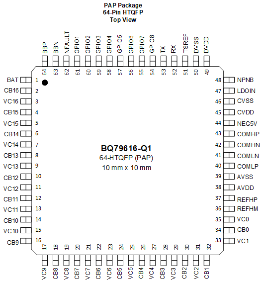
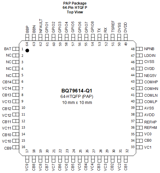
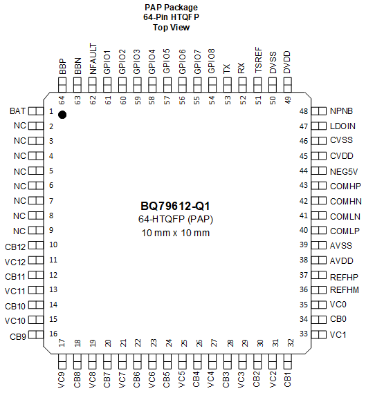
Table 7-1 Pin Functions
| PIN | TYPE | DESCRIPTION | |||
|---|---|---|---|---|---|
| NAME | No. | ||||
| BQ79616 | BQ79614 | BQ79612 | |||
| BAT | BAT | BAT | 1 | P | Power supply input and top of module measurement input. Connect to the top cell of the battery module. |
| NPNB | NPNB | NPNB | 48 | P | Connect to the base of an external NPN transistor. |
| LDOIN | LDOIN | LDOIN | 47 | P | 6-V preregulated analog power supply input/sense pin. Connect to the emitter of the external NPN transistor and connect a 0.1-µF decoupling capacitor to CVSS. |
| AVDD | AVDD | AVDD | 38 | P | 5-V regulated output. AVDD supplies the internal analog circuits. Bypass AVDD with a capacitor to AVSS. |
| AVSS | AVSS | AVSS | 39 | GND | Analog ground. Ground connection for internal analog circuits. Connect DVSS, CVSS, REFHM, and AVSS externally. |
| NEG5V | NEG5V | NEG5V | 44 | P | Negative 5-V charge pump used for daisy chain and Main ADC. Connect with a capacitor to CVSS. |
| DVDD | DVDD | DVDD | 49 | P | 1.8-V regulated output. DVDD supplies the internal digital circuits. Bypass DVDD with a capacitor to DVSS. |
| DVSS | DVSS | DVSS | 50 | GND | Digital ground. Ground connection for internal digital logics. Connect DVSS, CVSS, REFHM, and AVSS externally. |
| CVDD | CVDD | CVDD | 45 | P | 5-V daisy chain communication and I/Os power supply. CVDD supplies the stack daisy chain communication transceiver circuit and the I/O pins. This power supply also supports an additional 10-mA external load in ACTIVE and SLEEP. |
| CVSS | CVSS | CVSS | 46 | GND | Daisy chain communication ground. Ground connection for internal daisy chain transceivers. Connect DVSS, CVSS, REFHM, and AVSS externally. |
| TSREF | TSREF | TSREF | 51 | P | 5-V bias voltage for NTC thermistor. Connect TSREF to the top of the NTC resistor divider network to the GPIOs when they are configured for NTC temperature monitoring. Bypass TSREF with a capacitor to CVSS. |
| REFHP | REFHP | REFHP | 37 | P | Precision reference output pin. Bypass with a capacitor to REFHM. |
| REFHM | REFHM | REFHM | 36 | GND | Precision reference ground. Ground connection for the internal precision reference. Connect DVSS, CVSS, REFHM, and AVSS externally. |
| VC16 | NC | NC | 3 | I | Cell voltage sense input. Connect to the positive terminal of cell 16. Connect a differential RC filter to VC15. Tie unused NC pins in BQ79614 and BQ79612 to BAT pin as explained in Cell Connections. |
| VC15 | NC | NC | 5 | I | Cell voltage sense input. Connect to the positive terminal of cell 15. Connect a differential RC filter to VC14.Tie unused NC pins in BQ79614 and BQ79612 to BAT pin as explained in Cell Connections. |
| VC14 | VC14 | NC | 7 | I | Cell voltage sense input. Connect to the positive terminal of cell 14. Connect a differential RC filter to VC13.Tie unused NC pins in BQ79612 to BAT pin as explained in Cell Connections. |
| VC13 | VC13 | NC | 9 | I | Cell voltage sense input. Connect to the positive terminal of cell 13. Connect a differential RC filter to VC12. Tie unused NC pins in BQ79612 to BAT pin as explained in Cell Connections. |
| VC12 | VC12 | VC12 | 11 | I | Cell voltage sense input. Connect to the positive terminal of cell 12. Connect a differential RC filter to VC11. |
| VC11 | VC11 | VC11 | 13 | I | Cell voltage sense input. Connect to the positive terminal of cell 11. Connect a differential RC filter to VC10. |
| VC10 | VC10 | VC10 | 15 | I | Cell voltage sense input. Connect to the positive terminal of cell 10. Connect a differential RC filter to VC9. |
| VC9 | VC9 | VC9 | 17 | I | Cell voltage sense input. Connect to the positive terminal of cell 9. Connect a differential RC filter to VC8. |
| VC8 | VC8 | VC8 | 19 | I | Cell voltage sense input. Connect to the positive terminal of cell 8. Connect a differential RC filter to VC7. |
| VC7 | VC7 | VC7 | 21 | I | Cell voltage sense input. Connect to the positive terminal of cell 7. Connect a differential RC filter to VC6. |
| VC6 | VC6 | VC6 | 23 | I | Cell voltage sense input. Connect to the positive terminal of cell 6. Connect a differential RC filter to VC5. |
| VC5 | VC5 | VC5 | 25 | I | Cell voltage sense input. Connect to the positive terminal of cell 5. Connect a differential RC filter to VC4. |
| VC4 | VC4 | VC4 | 27 | I | Cell voltage sense input. Connect to the positive terminal of cell 4. Connect a differential RC filter to VC3. |
| VC3 | VC3 | VC3 | 29 | I | Cell voltage sense input. Connect to the positive terminal of cell 3. Connect a differential RC filter to VC2. |
| VC2 | VC2 | VC2 | 31 | I | Cell voltage sense input. Connect to the positive terminal of cell 2. Connect a differential RC filter to VC1. |
| VC1 | VC1 | VC1 | 33 | I | Cell voltage sense input. Connect to the positive terminal of cell 1. Connect a differential RC filter to VC0. |
| VC0 | VC0 | VC0 | 35 | I | Cell voltage sense input. Connect to the negative terminal of cell 1. Connect a differential RC filter to AVSS. |
| CB16 | NC | NC | 2 | I/O | Cell balance connection. This pin is connected to the internal cell balancing FET. Connect this pin to the positive terminal of cell 16 with a differential RC filter to CB15. The filter resistor also sets the internal balance current. Tie unused CB16 pin via RC to BAT pin and tie unused NC pins in BQ79614 and BQ79612 to BAT pin as explained in Cell Connections. |
| CB15 | NC | NC | 4 | I/O | Cell balance connection. This pin is connected to the internal cell balancing FET. Connect this pin to the positive terminal of cell 15 with a differential RC filter to CB14. The filter resistor also sets the internal balance current. Tie unused NC pins in BQ79614 and BQ79612 to BAT pin as explained in Cell Connections. |
| CB14 | CB14 | NC | 6 | I/O | Cell balance connection. This pin is connected to the internal cell balancing FET. Connect this pin to the positive terminal of cell 14 with a differential RC filter to CB13. The filter resistor also sets the internal balance current. Tie unused NC pins in BQ79612 to BAT pin as explained in Cell Connections. |
| CB13 | CB13 | NC | 8 | I/O | Cell balance connection. This pin is connected to the internal cell balancing FET. Connect this pin to the positive terminal of cell 13 with a differential RC filter to CB12. The filter resistor also sets the internal balance current. Tie unused NC pins in BQ79612 to BAT pin as explained in Cell Connections. |
| CB12 | CB12 | CB12 | 10 | I/O | Cell balance connection. This pin is connected to the internal cell balancing FET. Connect this pin to the positive terminal of cell 12 with a differential RC filter to CB11. The filter resistor also sets the internal balance current. |
| CB11 | CB11 | CB11 | 12 | I/O | Cell balance connection. This pin is connected to the internal cell balancing FET. Connect this pin to the positive terminal of cell 11 with a differential RC filter to CB10. The filter resistor also sets the internal balance current. |
| CB10 | CB10 | CB10 | 14 | I/O | Cell balance connection. This pin is connected to the internal cell balancing FET. Connect this pin to the positive terminal of cell 10 with a differential RC filter to CB9. The filter resistor also sets the internal balance current. |
| CB9 | CB9 | CB9 | 16 | I/O | Cell balance connection. This pin is connected to the internal cell balancing FET. Connect this pin to the positive terminal of cell 9 with a differential RC filter to CB8. The filter resistor also sets the internal balance current. |
| CB8 | CB8 | CB8 | 18 | I/O | Cell balance connection. This pin is connected to the internal cell balancing FET. Connect this pin to the positive terminal of cell 8 with a differential RC filter to CB7. The filter resistor also sets the internal balance current. |
| CB7 | CB7 | CB7 | 20 | I/O | Cell balance connection. This pin is connected to the internal cell balancing FET. Connect this pin to the positive terminal of cell 7 with a differential RC filter to CB6. The filter resistor also sets the internal balance current. |
| CB6 | CB6 | CB6 | 22 | I/O | Cell balance connection. This pin is connected to the internal cell balancing FET. Connect this pin to the positive terminal of cell 6 with a differential RC filter to CB5. The filter resistor also sets the internal balance current. |
| CB5 | CB5 | CB5 | 24 | I/O | Cell balance connection. This pin is connected to the internal cell balancing FET. Connect this pin to the positive terminal of cell 5 with a differential RC filter to CB4. The filter resistor also sets the internal balance current. |
| CB4 | CB4 | CB4 | 26 | I/O | Cell balance connection. This pin is connected to the internal cell balancing FET. Connect this pin to the positive terminal of cell 4 with a differential RC filter to CB3. The filter resistor also sets the internal balance current. |
| CB3 | CB3 | CB3 | 28 | I/O | Cell balance connection. This pin is connected to the internal cell balancing FET. Connect this pin to the positive terminal of cell 3 with a differential RC filter to CB2. The filter resistor also sets the internal balance current. |
| CB2 | CB2 | CB2 | 30 | I/O | Cell balance connection. This pin is connected to the internal cell balancing FET. Connect this pin to the positive terminal of cell 2 with a differential RC filter to CB1. The filter resistor also sets the internal balance current. |
| CB1 | CB1 | CB1 | 32 | I/O | Cell balance connection. This pin is connected to the internal cell balancing FET. Connect this pin to the positive terminal of cell 1 with a differential RC filter to CB0. The filter resistor also sets the internal balance current. |
| CB0 | CB0 | CB0 | 34 | I/O | Cell balance connection. This pin is connected to the internal cell balancing FET. Connect to the negative terminal of cell 1 with differential RC filter to AVSS. The filter resistor also sets the internal balance current. |
| BBP | BBP | BBP | 64 | I | Bus bar connection. With BBP and BBN connecting to each end of a bus bar, this channel provides a differential input to the ADC measurement with a 5x gain. |
| BBN | BBN | BBN | 63 | I | Bus bar connection. With BBP and BBN connecting to each end of a bus bar, this channel provides a differential input to the ADC measurement with a 5x gain. |
| RX | RX | RX | 52 | I | UART receiver input. Pull up to CVDD with an external resistor and connect the device RX to the TX output of the host MCU. If unused (for example, for stack devices), connect RX to CVDD. |
| TX | TX | TX | 53 | O | UART transmitter output. Connect device TX to RX input of the host MCU and will be pulled up from the host side. If unused (for example, for stack devices), leave it floating. |
| COMHP | COMHP | COMHP | 43 | I/O | Vertical bidirectional communication interface for daisy chain connection. High side (north side) differential I/O. Will connect to the low side (south side) COMLP and COMLN of the lower adjacent device in the daisy chain configuration. If unused, connect COMHP and COMHN with a 1kΩ resistor. |
| COMHN | COMHN | COMHN | 42 | I/O | |
| COMLP | COMLP | COMLP | 40 | I/O | Vertical bidirectional communication interface for daisy chain connection. Low side (south side) differential I/O. Will connect to the high side (north side) COMHP and COMHN of the upper adjacent device in the daisy chain configuration. If unused, connect COMLP and COMLN with a 1kΩ resistor. |
| COMLN | COMLN | COMLN | 41 | I/O | |
| NFAULT | NFAULT | NFAULT | 62 | O | Fault indication output. Active low. If used on the base device, pull up NFAULT to CVDD with a pullup resistor and connect NFAULT to host MCU GPIO. If unused, leave it unconnected. |
| GPIO1 | GPIO1 | GPIO1 | 61 | I/O | General purpose input/output,
configuration options are:
|
| GPIO2 | GPIO2 | GPIO2 | 60 | I/O | |
| GPIO3 | GPIO3 | GPIO3 | 59 | I/O | |
| GPIO4 | GPIO4 | GPIO4 | 58 | I/O | |
| GPIO5 | GPIO5 | GPIO5 | 57 | I/O | |
| GPIO6 | GPIO6 | GPIO6 | 56 | I/O | |
| GPIO7 | GPIO7 | GPIO7 | 55 | I/O | |
| GPIO8 | GPIO8 | GPIO8 | 54 | I/O | |