ZHCS926C May 2012 – May 2021 BQ34Z100
PRODUCTION DATA
- 1 特性
- 2 应用
- 3 说明
- 4 Revision History
- 5 Pin Configuration and Functions
-
6 Specifications
- 6.1 Absolute Maximum Ratings
- 6.2 ESD Ratings
- 6.3 Recommended Operating Conditions
- 6.4 Thermal Information
- 6.5 Electrical Characteristics: Power-On Reset
- 6.6 Electrical Characteristics: LDO Regulator
- 6.7 Electrical Characteristics: Internal Temperature Sensor Characteristics
- 6.8 Electrical Characteristics: Low-Frequency Oscillator
- 6.9 Electrical Characteristics: High-Frequency Oscillator
- 6.10 Electrical Characteristics: Integrating ADC (Coulomb Counter) Characteristics
- 6.11 Electrical Characteristics: ADC (Temperature and Cell Measurement) Characteristics
- 6.12 Electrical Characteristics: Data Flash Memory Characteristics
- 6.13 Timing Requirements: HDQ Communication
- 6.14 Timing Requirements: I2C-Compatible Interface
- 6.15 Typical Characteristics
-
7 Detailed Description
- 7.1 Overview
- 7.2
Feature Description
- 7.2.1
Data Commands
- 7.2.1.1 Standard Data Commands
- 7.2.1.2
Control(): 0x00/0x01
- 7.2.1.2.1 CONTROL_STATUS: 0x0000
- 7.2.1.2.2 DEVICE TYPE: 0x0001
- 7.2.1.2.3 FW_VERSION: 0x0002
- 7.2.1.2.4 HW_VERSION: 0x0003
- 7.2.1.2.5 RESET_DATA: 0x0005
- 7.2.1.2.6 PREV_MACWRITE: 0x0007
- 7.2.1.2.7 CHEM ID: 0x0008
- 7.2.1.2.8 BOARD_OFFSET: 0x0009
- 7.2.1.2.9 CC_OFFSET: 0x000A
- 7.2.1.2.10 CC_OFFSET_SAVE: 0x000B
- 7.2.1.2.11 DF_VERSION: 0x000C
- 7.2.1.2.12 SET_FULLSLEEP: 0x0010
- 7.2.1.2.13 STATIC_CHEM_DF_CHKSUM: 0x0017
- 7.2.1.2.14 SEALED: 0x0020
- 7.2.1.2.15 IT ENABLE: 0x0021
- 7.2.1.2.16 RESET: 0x0041
- 7.2.1.2.17 EXIT_CAL: 0x0080
- 7.2.1.2.18 ENTER_CAL: 0x0081
- 7.2.1.2.19 OFFSET_CAL: 0x0082
- 7.2.1.3 StateOfCharge(): 0x02/0x03
- 7.2.1.4 RemainingCapacity(): 0x04/0x05
- 7.2.1.5 FullChargeCapacity(): 0x06/07
- 7.2.1.6 Voltage(): 0x08/0x09
- 7.2.1.7 AverageCurrent(): 0x0A/0x0B
- 7.2.1.8 Temperature(): 0x0C/0x0D
- 7.2.1.9 Flags(): 0x0E/0x0F
- 7.2.2
Extended Data Commands
- 7.2.2.1 AtRate(): 0X10/0x11
- 7.2.2.2 AtRateTimeToEmpty(): 0x12/0x13
- 7.2.2.3 Current(): 0x10/0x11
- 7.2.2.4 NominalAvailableCapacity(): 0x14/0x15
- 7.2.2.5 FullAvailableCapacity(): 0x16/0x17
- 7.2.2.6 TimeToEmpty(): 0x18/0x19
- 7.2.2.7 TimeToFull(): 0x1A/0x1B
- 7.2.2.8 StandbyCurrent(): 0x1C/0x1D
- 7.2.2.9 StandbyTimeToEmpty(): 0x1E/0x1F
- 7.2.2.10 MaxLoadCurrent(): 0x20/0x21
- 7.2.2.11 MaxLoadTimeToEmpty(): 0x22/0x23
- 7.2.2.12 AvailableEnergy(): 0x24/0x25
- 7.2.2.13 AveragePower(): 0x26/0x27
- 7.2.2.14 TimeToEmptyAtConstantPower(): 0x28/0x29
- 7.2.2.15 InternalTemp(): 0x2A/0x2B
- 7.2.2.16 CycleCount(): 0x2C/0x2D
- 7.2.2.17 StateOfHealth(): 0x2E/0x2F
- 7.2.2.18 ChargeVoltage(): 0x30/0x31
- 7.2.2.19 ChargeCurrent(): 0x32/0x33
- 7.2.2.20 PassedCharge(): 0x34/0x35
- 7.2.2.21 DOD0(): 0x36/0x37
- 7.2.2.22 SelfDischargeCurrent(): 0x38/0x39
- 7.2.2.23 PackConfiguration(): 0x3A/0x3B
- 7.2.2.24 DesignCapacity(): 0x3C/0x3D
- 7.2.2.25 DataFlashClass(): 0x3E
- 7.2.2.26 DataFlashBlock(): 0x3F
- 7.2.2.27 AuthenticateData/BlockData(): 0x40…0x53
- 7.2.2.28 AuthenticateChecksum/BlockData(): 0x54
- 7.2.2.29 BlockData(): 0x55…0x5F
- 7.2.2.30 BlockDataChecksum(): 0x60
- 7.2.2.31 BlockDataControl(): 0x61
- 7.2.2.32 DeviceNameLength(): 0x62
- 7.2.2.33 DeviceName(): 0x63…0x6A
- 7.2.3 Data Flash Interface
- 7.2.4 Data Flash Summary
- 7.2.5 Fuel Gauging
- 7.2.6
Impedance Track Variables
- 7.2.6.1 Load Mode
- 7.2.6.2 Load Select
- 7.2.6.3 Reserve Cap-mAh
- 7.2.6.4 Reserve Cap-mWh/cWh
- 7.2.6.5 Design Energy Scale
- 7.2.6.6 Dsg Current Threshold
- 7.2.6.7 Chg Current Threshold
- 7.2.6.8 Quit Current, Dsg Relax Time, Chg Relax Time, and Quit Relax Time
- 7.2.6.9 Qmax
- 7.2.6.10 Update Status
- 7.2.6.11 Avg I Last Run
- 7.2.6.12 Avg P Last Run
- 7.2.6.13 Delta Voltage
- 7.2.6.14 Ra Tables
- 7.2.6.15 Pack Configuration Register
- 7.2.7 Voltage Division and Calibration
- 7.2.8 Temperature Measurement
- 7.2.9 Overtemperature Indication
- 7.2.10 Charging and Charge Termination Indication
- 7.2.11 X10 Mode
- 7.2.12 Remaining State of Charge LED Indication
- 7.2.13 Alert Signal
- 7.2.14 Communications
- 7.2.15 Power Control
- 7.2.1
Data Commands
- 7.3 Device Functional Modes
-
8 Application and Implementation
- 8.1
Typical Applications
- 8.1.1 Design Requirements
- 8.1.2
Detailed Design Procedure
- 8.1.2.1
Step-by-Step Design Procedure
- 8.1.2.1.1 STEP 1: Review and Modify the Data Flash Configuration Data.
- 8.1.2.1.2 STEP 2: Review and Modify the Data Flash Configuration Registers.
- 8.1.2.1.3 STEP 3: Design and Configure the Voltage Divider.
- 8.1.2.1.4 STEP 4: Determine the Sense Resistor Value.
- 8.1.2.1.5 STEP 5: Review and Modify the Data Flash Gas Gauging Configuration, Data, and State.
- 8.1.2.1.6 STEP 6: Determine and Program the Chemical ID.
- 8.1.2.1.7 STEP 7: Calibrate.
- 8.1.2.1.8 STEP 8: Run an Optimization Cycle.
- 8.1.2.1
Step-by-Step Design Procedure
- 8.1.3 Battery Chemistry Configuration
- 8.1.4 Replaceable Battery Systems
- 8.1.5 Digital Interface Options
- 8.1.6 Display Options
- 8.1.7 Application Curves
- 8.1.8 Special Applications
- 8.1
Typical Applications
- 9 Power Supply Recommendations
- 10Layout
- 11Device and Documentation Support
- 12Mechanical, Packaging, and Orderable Information
9 Power Supply Recommendations
Power supply requirements for the BQ34Z100 are simplified due to the presence of the internal LDO voltage regulation. The REGIN pin accepts any voltage level between 2.7 V and 4.5 V, which is optimum for a single-cell Li-ion application. For higher battery voltage applications, a simple pre-regulator can be provided to power the bq34Z100 and any optional LEDs. Decoupling the REGIN pin should be done with a 0.1-µF 10% ceramic X5R capacitor placed close to the device. While the pre-regulator circuit is not critical, special attention should be paid to its quiescent current and power dissipation. The input voltage should handle the maximum battery stack voltage. The output voltage can be centered within the 2.7-V to 4.5-V range as recommended for the REGIN pin.
For high stack count applications, a commercially available LDO is often the best quality solution, but comes with a cost tradeoff. To lower the BOM cost, the following approaches are recommended.
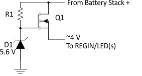
In Figure 9-1, Q1 is used to drop the battery stack voltage to roughly 4 V to power the BQ34Z100 REGIN pin and also to feed the anode of any LEDs used in the application. To avoid unwanted quiescent current consumption, R1 should be set as high as is practical. It is recommended to use a low-current Zener diode.
 Figure 9-1 Q1 Dropping Battery Stack
Voltage to 4 V
Figure 9-1 Q1 Dropping Battery Stack
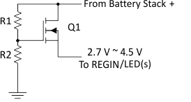
Voltage to 4 VAlternatively, if the range of a high-voltage battery stack can be well defined, a simple source follower based on a resistive divider can be used to lower the BOM cost and the quiescent current. For example:
 Figure 9-2 Source Follower on a
Resistive Divider
Figure 9-2 Source Follower on a
Resistive DividerPower dissipation of the linear pre-regulator may become an important design decision when multiple LEDs are employed in the application. For example, the BQ34Z100 EVM uses a pair of FETs in parallel to inexpensively dissipate enough power for 10-LED evaluation.