ZHCSLK7A july 2020 – april 2023 BQ21062
PRODUCTION DATA
- 1
- 1 特性
- 2 应用
- 3 说明
- 4 Revision History
- 5 说明(续)
- 6 Device Comparison Table
- 7 Pin Configuration and Functions
- 8 Specifications
-
9 Detailed Description
- 9.1 Overview
- 9.2 Functional Block Diagram
- 9.3
Feature Description
- 9.3.1 Linear Charger and Power Path
- 9.3.2 Protection Mechanisms
- 9.3.3 VDD LDO
- 9.3.4 Load Switch/LDO Output and Control
- 9.3.5 PMID Power Control
- 9.3.6 System Voltage (PMID) Regulation
- 9.3.7 MR Wake and Reset Input
- 9.3.8 14-Second Watchdog for HW Reset
- 9.3.9 Faults Conditions and Interrupts ( INT)
- 9.3.10 Power Good ( PG) Pin
- 9.3.11 External NTC Monitoring (TS)
- 9.3.12 I2C Interface
- 9.4 Device Functional Modes
- 9.5 Register Map
- 10Application and Implementation
- 11Power Supply Recommendations
- 12Layout
- 13Device and Documentation Support
- 14Mechanical, Packaging, and Orderable Information
9.3.1.1 Battery Charging Process
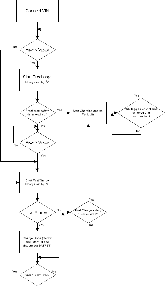
The following diagram summarizes the charging process of the BQ21062 charger.
 Figure 9-1 BQ21062 Charger Flow Diagram
When a valid input source is connected (VIN > VUVLO and VBAT+VSLP < VIN < VOVP), the state of the CE pin determines whether a charge cycle is initiated. When the CE input is high and a valid input source is connected, the battery charge FET is turned off, preventing any kind of charging of the battery. A charge cycle is initiated when the CHARGE_DISABLE bit is written to 0 and CE pin in low. Table 9-1 shows the CE pin and bit priority to enable/disable charging.
| CE PIN | CHARGE _DISABLE BIT | CHARGING |
|---|---|---|
| 0 | 0 | Enabled |
| 0 | 1 | Disabled |
| 1 | 0 | Disabled |
| 1 | 1 | Disabled |
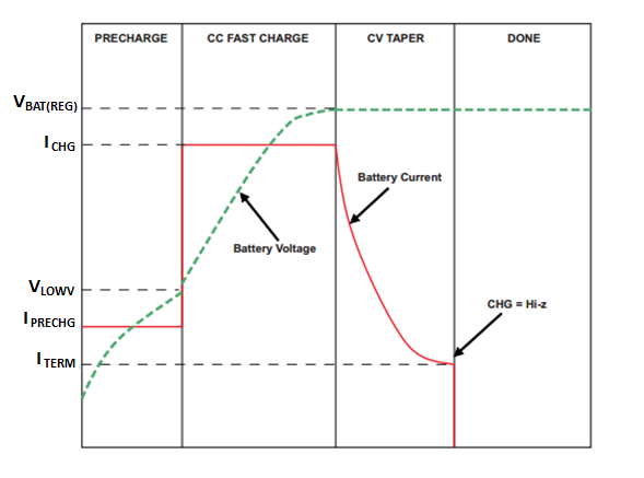
Figure 9-2 shows a typical charge cycle.
 Figure 9-2 BQ21062 Typical Charge Cycle
During Pre-Charge, where the battery voltage is below the VLOWV level, the battery willl be charge with IPRECHARGE current which can be programmed through I2C. During pre-charge, the safety timer is set to 25% of the safety timer value during fast charge. Once the battery voltage reaches VLOWV, the charger will then operate in Fast Charge Mode, charging the battery at ICHARGE which may also be programmed through I2C. Once the battery voltage approaches the VBATREG level, the charging current starts tapering off as shown in Figure 9-2. Once the charging current reaches the termination current (ITERM) charging is stopped. Note that to ensure that the battery is charged to VBATREG level, the regulated PMID voltage should be set to at least 200mV above VBATREG. Termination is only enabled when the charger CV loop is active in fast charge operation. No termination will occur if the charge current reaches ITERM while VINDPM is active as well as the thermal regulation loop. Termination is also disabled when operating in the TS WARM region. The charger only goes to termination when the current drops to ITERM due to the battery reaching the target voltage and not due to the charge current limitation imposed by the previously mentioned control loops
Whenever a change in the charge current setting is triggered, whether it occurs due to I2C programming by the host, Pre-Charge/Fast Charge transition or JEITA TS control, the device will temporarily disable charging (for ~ 1 ms) before updating the charge current value.