ZHCSH75A September   2017  – December 2017 ADS7142

PRODUCTION DATA.  

  1. 特性
  2. 应用
  3. 说明
    1.     Device Images
  4. 修订历史记录
  5. Pin Configuration and Functions
    1.     Pin Functions
  6. Specifications
    1. 6.1  Absolute Maximum Ratings
    2. 6.2  ESD Ratings
    3. 6.3  Recommended Operating Conditions
    4. 6.4  Thermal Information
    5. 6.5  Electrical Characteristics - All Modes
    6. 6.6  Electrical Characteristics - Manual Mode
    7. 6.7  Electrical Characteristics - Autonomous Modes
    8. 6.8  Electrical Characteristics - High Precision Mode
    9. 6.9  Timing Requirements
    10. 6.10 Switching Characteristics
    11. 6.11 Typical Characteristics for All Modes
    12. 6.12 Typical Characteristics for Manual Mode
    13. 6.13 Typical Characteristics for Autonomous Modes
    14. 6.14 Typical Characteristics for High Precision Mode
  7. Detailed Description
    1. 7.1 Overview
    2. 7.2 Functional Block Diagram
    3. 7.3 Feature Description
      1. 7.3.1  Analog Input and Multiplexer
        1. 7.3.1.1 Two-Channel, Single-Ended Configuration
        2. 7.3.1.2 Single-Channel, Single-Ended Configuration
        3. 7.3.1.3 Single-Channel, Pseudo-Differential Configuration
      2. 7.3.2  OFFSET Calibration
      3. 7.3.3  Reference
      4. 7.3.4  ADC Transfer Function
      5. 7.3.5  Oscillator and Timing Control
      6. 7.3.6  I2C Address Selector
      7. 7.3.7  Data Buffer
        1. 7.3.7.1 Filling of the Data Buffer
        2. 7.3.7.2 Reading data from the Data Buffer
      8. 7.3.8  Accumulator
      9. 7.3.9  Digital Window Comparator
      10. 7.3.10 I2C Protocol Features
        1. 7.3.10.1 General Call
        2. 7.3.10.2 General Call with Software Reset
        3. 7.3.10.3 General Call with Write Software programmable part of slave address
        4. 7.3.10.4 Configuring Device into High Speed I2C mode
        5. 7.3.10.5 Bus Clear
      11. 7.3.11 Device Programming
        1. 7.3.11.1 Reading Registers
          1. 7.3.11.1.1 Single Register Read
          2. 7.3.11.1.2 Reading a Continuous Block of Registers
        2. 7.3.11.2 Writing Registers
          1. 7.3.11.2.1 Single Register Write
          2. 7.3.11.2.2 Set Bit
          3. 7.3.11.2.3 Clear Bit
          4. 7.3.11.2.4 Writing a continuous block of registers
    4. 7.4 Device Functional Modes
      1. 7.4.1 Device Power Up and Reset
      2. 7.4.2 Manual Mode
        1. 7.4.2.1 Manual Mode with CH0 Only
        2. 7.4.2.2 Manual Mode with AUTO Sequence
      3. 7.4.3 Autonomous Modes
        1. 7.4.3.1 Autonomous Mode with Threshold Monitoring and Diagnostics
          1. 7.4.3.1.1 Autonomous Mode with Pre Alert Data
          2. 7.4.3.1.2 Autonomous Mode with Post Alert Data
        2. 7.4.3.2 Autonomous Mode with Burst Data
          1. 7.4.3.2.1 Autonomous Mode with Start Burst
          2. 7.4.3.2.2 Autonomous Mode with Stop Burst
      4. 7.4.4 High Precision Mode
    5. 7.5 Optimizing Power Consumed by the Device
    6. 7.6 Register Map
      1. 7.6.1 RESET REGISTERS
        1. 7.6.1.1 WKEY Register (address = 17h), [reset = 00h]
          1. Table 6. WKEY Register Field Descriptions
        2. 7.6.1.2 DEVICE_RESET Register (address = 14h), [reset = 00h]
          1. Table 7. DEVICE_RESET Register Field Descriptions
      2. 7.6.2 FUNCTIONAL MODE SELECT REGISTERS
        1. 7.6.2.1 OFFSET_CAL Register (address = 15h), [reset = 00h]
          1. Table 8. OFFSET_CAL Register Field Descriptions
        2. 7.6.2.2 OPMODE_SEL Register (address = 1Ch), [reset = 00h]
          1. Table 9. OPMODE_SEL Register Field Descriptions
        3. 7.6.2.3 OPMODE_I2CMODE_STATUS Register (address = 00h), [reset = 00h]
          1. Table 10. OPMODE_I2CMODE_STATUS Register Field Descriptions
      3. 7.6.3 INPUT CONFIG REGISTER
        1. 7.6.3.1 CHANNEL_INPUT_CFG Register (address = 24h), [reset = 00h]
          1. Table 11. CHANNEL_INPUT_CFG Register Field Descriptions
      4. 7.6.4 ANALOG MUX and SEQUENCER REGISTERS
        1. 7.6.4.1 AUTO_SEQ_CHEN Register (address = 20h), [reset = 03h]
          1. Table 12. AUTO_SEQ_CHEN Register Field Descriptions
        2. 7.6.4.2 START_SEQUENCE Register (address = 1Eh), [reset = 00h]
          1. Table 13. START_SEQUENCE Register Field Descriptions
        3. 7.6.4.3 ABORT_SEQUENCE Register (address = 1Fh), [reset = 00h]
          1. Table 14. ABORT_SEQUENCE Register Field Descriptions
        4. 7.6.4.4 SEQUENCE_STATUS Register (address = 04h), [reset = 00h]
          1. Table 15. SEQUENCE_STATUS Register Field Descriptions
      5. 7.6.5 OSCILLATOR and TIMING CONTROL REGISTERS
        1. 7.6.5.1 OSC_SEL Register (address = 18h), [reset = 00h]
          1. Table 16. OSC_SEL Register Field Descriptions
        2. 7.6.5.2 nCLK_SEL Register (address = 19h), [reset = 00h]
          1. Table 17. nCLK_SEL Register Field Descriptions
      6. 7.6.6 DATA BUFFER CONTROL REGISTER
        1. 7.6.6.1 DATA_BUFFER_OPMODE Register (address = 2Ch), [reset = 01h]
          1. Table 18. DATA_BUFFER_OPMODE Register Field Descriptions
        2. 7.6.6.2 DOUT_FORMAT_CFG Register (address = 28h), [reset = 00h]
          1. Table 19. DOUT_FORMAT_CFG Register Field Descriptions
        3. 7.6.6.3 DATA_BUFFER_STATUS Register (address = 01h), [reset = 00h]
          1. Table 20. DATA_BUFFER_STATUS Register Field Descriptions
      7. 7.6.7 ACCUMULATOR CONTROL REGISTERS
        1. 7.6.7.1 ACC_EN Register (address = 30h), [reset = 00h]
          1. Table 21. ACC_EN Register Field Descriptions
        2. 7.6.7.2 ACC_CH0_LSB Register (address = 08h), [reset = 00h]
          1. Table 22. ACC_CH0_LSB Register Field Descriptions
        3. 7.6.7.3 ACC_CH0_MSB Register (address = 09h), [reset = 00h]
          1. Table 23. ACC_CH0_MSB Register Field Descriptions
        4. 7.6.7.4 ACC_CH1_LSB Register (address = 0Ah), [reset = 00h]
          1. Table 24. ACC_CH1 LSB Register Field Descriptions
        5. 7.6.7.5 ACC_CH1_MSB Register (address = 0Bh), [reset = 00h]
          1. Table 25. ACC_CH1 MSB Register Field Descriptions
        6. 7.6.7.6 ACCUMULATOR_STATUS Register (address = 02h), [reset = 00h]
          1. Table 26. ACCUMULATOR_STATUS Register Field Descriptions
      8. 7.6.8 DIGITAL WINDOW COMPARATOR REGISTERS
        1. 7.6.8.1  ALERT_DWC_EN Register (address = 37h), [reset = 00h]
          1. Table 27. ALERT_DWC_EN Register Field Descriptions
        2. 7.6.8.2  ALERT_CHEN (address = 34h), [reset = 00h]
          1. Table 28. ALERT_CHEN Register Field Descriptions
        3. 7.6.8.3  DWC_HTH_CH0_MSB Register (address = 39h), [reset = 00h]
          1. Table 29. DWC_HTH_CH0_LSB Register Field Descriptions
        4. 7.6.8.4  DWC_HTH_CH0_LSB Register (address = 38h), [reset = 00h]
          1. Table 30. DWC_HTH_CH0_LSB Register Field Descriptions
        5. 7.6.8.5  DWC_LTH_CH0_MSB Register (address = 3Bh), [reset = 00h]
          1. Table 31. DWC_LTH_CH0_MSB Register Field Descriptions
        6. 7.6.8.6  DWC_LTH_CH0_LSB Register (address = 3Ah), [reset = 00h]
          1. Table 32. DWC_LTH_CH0_LSB Register Field Descriptions
        7. 7.6.8.7  DWC_HYS_CH0 (address = 40h), [reset = 00h]
          1. Table 33. DWC_HYS_CH0 Register Field Descriptions
        8. 7.6.8.8  DWC_HTH_CH1_MSB Register (address = 3Dh), [reset = 00h]
          1. Table 34. DWC_HTH_CH1_LSB Register Field Descriptions
        9. 7.6.8.9  DWC_HTH_CH1_LSB Register (address = 3Ch), [reset = 00h]
          1. Table 35. DWC_HTH_CH1_LSB Register Field Descriptions
        10. 7.6.8.10 DWC_LTH_CH1_MSB Register (address = 3Fh), [reset = 00h]
          1. Table 36. DWC_LTH_CH1_MSB Register Field Descriptions
        11. 7.6.8.11 DWC_LTH_CH1_LSB Register (address = 3Eh), [reset = 00h]
          1. Table 37. DWC_LTH_CH1_LSB Register Field Descriptions
        12. 7.6.8.12 DWC_HYS_CH1 (address = 41h), [reset = 00h]
          1. Table 38. DWC_HYS_CH1 Register Field Descriptions
        13. 7.6.8.13 PRE_ALT_MAX_EVENT_COUNT Register (address = 36h), [reset = 00h]
          1. Table 39. PRE_ALT_MAX_EVENT_COUNT Register Field Descriptions
        14. 7.6.8.14 ALERT_TRIG_CHID Register (address = 03h), [reset = 00h]
          1. Table 40. ALERT_TRIG_CHID Register Field Descriptions
        15. 7.6.8.15 ALERT_LOW_FLAGS Register (address = 0C), [reset = 00h]
          1. Table 41. ALERT_LOW_FLAGS Register Field Descriptions
        16. 7.6.8.16 ALERT_HIGH_FLAGS Register (address = 0Eh), [reset = 00h]
          1. Table 42. ALERT_HIGH_FLAGS Register Field Descriptions
  8. Application and Implementation
    1. 8.1 Application Information
    2. 8.2 Typical Applications
      1. 8.2.1 ADS7142 as a Programmable Comparator with False Trigger Prevention and Diagnostics
        1. 8.2.1.1 Design Requirements
          1. 8.2.1.1.1 Higher Power Consumption
          2. 8.2.1.1.2 Fixed Threshold Voltages
        2. 8.2.1.2 Detailed Design Procedure
          1. 8.2.1.2.1 Programmable Thresholds and Hysteresis
          2. 8.2.1.2.2 False Trigger Prevention with Event Counter
          3. 8.2.1.2.3 Fault Diagnostics with Data Buffer
        3. 8.2.1.3 Application Curve
      2. 8.2.2 Event-triggered PIR sensing with ADS7142
        1. 8.2.2.1 Design Requirements
        2. 8.2.2.2 Detailed Design Procedure
        3. 8.2.2.3 Application Curves
  9. Power-Supply Recommendations
    1. 9.1 AVDD and DVDD Supply Recommendations
  10. 10Layout
    1. 10.1 Layout Guidelines
    2. 10.2 Layout Example
  11. 11器件和文档支持
    1. 11.1 文档支持
    2. 11.2 接收文档更新通知
    3. 11.3 社区资源
    4. 11.4 商标
    5. 11.5 静电放电警告
    6. 11.6 Glossary
  12. 12机械、封装和可订购信息

封装选项

机械数据 (封装 | 引脚)
散热焊盘机械数据 (封装 | 引脚)
订购信息

Autonomous Modes

In Autonomous Mode, the device can be programmed to monitor the voltage applied on the analog input pins of the device and generate a signal on the ALERT pin when the programmable high or low threshold values are crossed and store the conversion results in the data buffer before or after the crossing a threshold or before setting the SEQ_ABORT bit (Start Burst) or after setting the START_SEQUENCE bit.

In Autonomous mode, the device generates the start of conversion using the internal oscillator. The first start of conversion must be provided by the host and the device generates the subsequent start of conversions.

After configuring the operation mode to autonomous mode (Set OPMODE_SEL register to 110b) as illustrated in Figure 54, steps for operating the device to be in different autonomous modes are illustrated in Figure 57
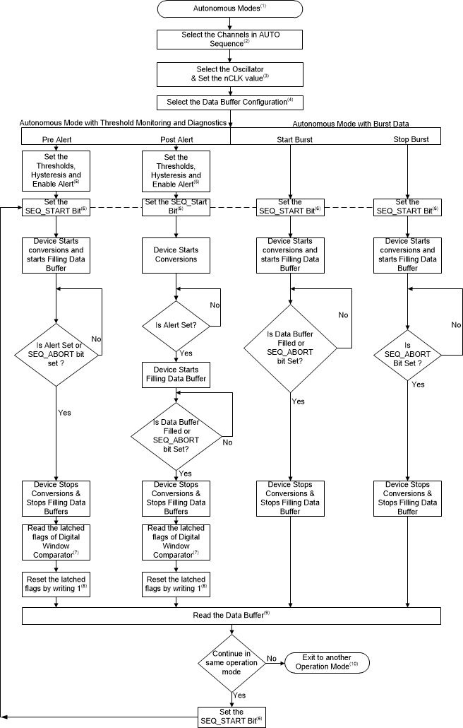
ADS7142 fc_autonomous_mode_BAS773.gif
For setting the operation mode to Autonomous modes, Refer to Figure 54
Select channels in the AUTO_SEQ_CFG register.
Select the oscillator by configuring the OSC_SEL register and configure the nCLK register.
Select the data buffer mode in the DATA_BUFFER_OPMODE register.
Configure the thresholds in the DWC_xTH_CHx_xxx registers and hysteresis in the DWC_HYS_CHx registers. Enable the alert for channels in the ALERT_CHEN register and set the DWC_BLOCK_EN bit in the ALERT_DWC_EN register.
Set the bit SEQ_START bit in the START_SEQUENCE register.
Read the ALERT_LOW_FLAGS and/or ALERT_HIGH_FLAGS registers.
Reset the ALERT_LOW_FLAGS and/or ALERT_HIGH_FLAGS registers by writing 03h.
Select another operation mode in the OPMODE_SEL register.
For reading and writing registers, Refer to Device Programming section.
Figure 57. Configuring Device in Autonomous Modes

TI recommends aborting the present sequence by setting the SEQ_ABORT bit before changing the device operation mode or device configuration.